


Wafer Probing Equipment for Device Characterization
Key Features
- Highly configurable wafer probing equipment for device characterization
- Manual, semiautomatic and fully automatic versions
- Customized according to users exact probing requirements
- Integrate thermal chucks, cooled and shielded chambers etc.
- Measure DC, IV/CV, Capacitance, HF, 1/f, temperature and more
- Specific drivers support integration of advanced instrumentation
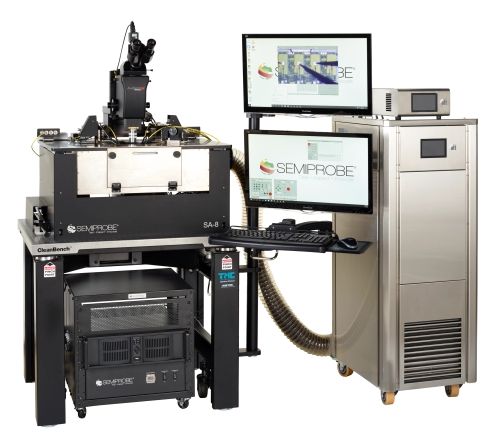
SemiProbe manufactures application specific wafer probing equipment for device characterization with the ability to make multiple types of measurements, in either manual, semiautomatic or fully automatic configurations. The systems are highly configurable for testing packaged parts, die, and small samples, through to 300mm wafers.
Options include thermal chucks for testing at elevated or cooled temperatures, shielding for light, thermal or measurement requirements. Systems can also be integrated with a wide range of third party equipment, whilst test instruments can be connected using probe cards and manual or programmable manipulators.
Full driver libraries are available for LabView, C++, and Visual Basic, with specific instrument drivers to support the most advanced instrumentation available. Communications may be made using RS-232, GPIB or TCP/IP, enabling the system to be either a controller or a slave in an integrated solution.
SemiProbe’s device characterization wafer probing equipment is configured using their patented Probe System for Life™ (PS4L) adaptive architecture. This modular concept enables seamless integration of advanced capabilities to deliver precise, accurate, repeatable measurements on even the most sophisticated semiconductor devices.


Wafer Probing Equipment Downloads
File
SemiProbe Corporate Overview Datasheet
Download
Example Applications
Semiautomatic Probe Station for Characterization
More
Fully Automatic Probe Station for Characterization

More
Related Products
Manual Probe Stations

More
Semiautomatic Wafer Probers

More
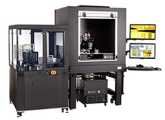
Fully Automatic Wafer Probers
More
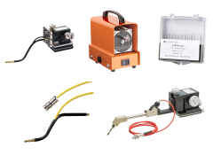
Wafer Probe Accessories
More
Semiconductor Wafers

More
Knowledge Base Articles
Description
Description
Glossary of Probing Terms and Acronyms
Link
Description
What is a Probe Station and How Does it Work?
Link
Description
Wafer Probe Tip Selection (IKB-034)
Link
Description
Probe Station Manipulator Overview (IKB-055)
Link
Description
Probe Station Wafer Chuck Guide (IKB-056)
Link
Further Information
Applications
Testing MEMS, MOEMS, NEMS, Sensors, Micro-bolometers, Gyros, Microfluidics etc.
Industry Segments
University Research, Development, Characterisation, MEMS Production Test
SemiProbe Website
Region
Europe, including: Austria, Belgium, Bulgaria, Czechia, Denmark, Finland, France, Germany, Ireland, Italy, Netherlands, Norway, Poland, Spain, Sweden, Slovakia, Switzerland, Türkiye, United Kingdom, etc.
Request Form
 Back to top