
Semiconductor Wafer Division
Inseto is a leading UK-based semiconductor wafer and substrate supplier, proudly supporting customers worldwide in research, academia, and high-tech manufacturing. We supply a comprehensive range of high-quality wafer materials that meet strict standards for flatness, cleanliness, and crystal orientation. These include:
- Silicon Wafers – Prime, test, and mechanical grade
- Silicon Oxide Wafers – SiO₂ wafer coatings
- Silicon Nitride Wafers – Si₃N₄ wafer coatings
- Glass & Fused Silica Wafers – Ideal for photonics and microfluidics
- Silicon-on-Insulator (SOI) – For advanced device & MEMS fabrication
- Silicon-on-Sapphire (SOS) – Specialised substrates for thermal and optical environments
- Sapphire – High-purity substrates for thermal and optical environments
- Compound Semiconductor Wafers – Including SiC, InP, GaN, GaAs and Ge
For applications requiring oxide or nitride coatings, our silicon wafers can be processed using atmospheric thermal oxide: dry oxide (for thinner layers); wet oxide (for thicker layers) or PECVD oxide (when single-sided coatings are required). Additionally, for nitride coatings, we offer PECVD, LPCVD, or low-stress LPCVD options.
Inseto also provides a range of additional fabrication processes to tailor wafers to your exact requirements. These include thinning, plating, bumping with solder or copper pillars, and dicing to virtually any die size.
All wafers are available in SEMI standard, PRIME, TEST, and custom thicknesses, with single or double-side polish and full traceability via Certificates of Conformance and compliance with industry standards.
Get in touch with enquiries about our range of semiconductor wafers
Send us an enquiry
Close

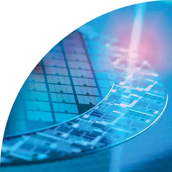
Explore the Range of Semiconductor Wafers


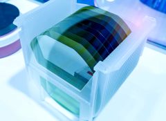
Get Expert Advice on Choosing the Right Wafer
Need help choosing the right wafer? Our team is ready to assist with expert guidance and custom solutions.
To get in touch: enquiries@inseto.com or call: +44 1264 334505
Further Semiconductor Wafer Information
Inseto Semiconductor Wafer Product Overview
Semiconductor Wafer Training Course
Wiki – Semiconductor Wafer Description
Discover our Semiconductor Wafer Knowledge Base Information
Please visit Inseto’s online Knowledge Base to view documentation on Semiconductor Wafer Selection and Wafer Nomenclature. Alternatively, contact us to find out more about our Wafer Training Courses, which can be held online or onsite and are designed to assist with wafer selection and material suitability for specific applications.
Semiconductor Wafer Training Course
For a deeper dive into semiconductor wafers contact us to find out more about our Wafer Training Courses, which can be held online or onsite and are designed to assist with wafer selection and material suitability for specific applications.
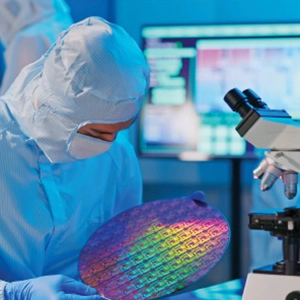
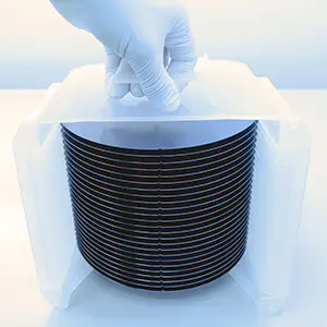
Shop Online for Semiconductor Wafers
We maintain a large inventory of standard wafer types for rapid dispatch. Browse our online semiconductor wafer store to view current stock and technical specifications, and to buy wafers online.
- Extensive Product Range: A wide selection wafer sizes & thicknesses
- Fast Global Shipping: Rapid dispatch from our production or UK warehouse
- Custom Processing: Oxide and nitride deposition, wafer thinning and more
- Expert Support: Technical advice to help you select the right wafer
- No Minimum Order: Perfect for both R&D and production environments
- Quality Assurance: All wafers undergo rigorous inspection processes
What is a Semiconductor Wafer?
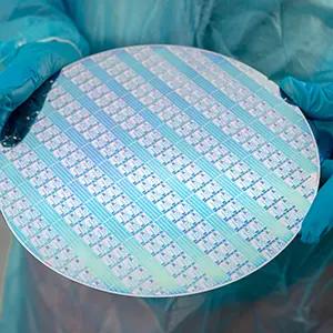
A semiconductor wafer is a thin, flat disc made from a material whose electrical conductivity falls between that of a conductor (e.g., copper) and an insulator (e.g., glass). It serves as the substrate for building electronic components such as diodes, transistors, and integrated circuits (ICs), forming the foundation of modern electronics.
Materials used to make Semiconductor Wafers
The most widely used material is Silicon (Si), with other materials chosen for specialised applications. Each material has different mechanical strength, thermal stability, and electrical characteristics. The most common semiconductor wafers and substrate materials comprise:
- Silicon (Si): Most widely used; excellent electrical properties and low cost.
- Germanium (Ge): High electron mobility; used in high-speed devices.
- Gallium Arsenide (GaAs): Superior frequency response; used in HF devices.
- Silicon Carbide (SiC): High thermal conductivity; ideal for power electronics.
- Gallium Nitride (GaN): High efficiency and power density; for HF & LEDs.
- Indium Phosphide (InP): Direct bandgap & high mobility, ideal for optoelectronics.
- Lithium Niobate (LiNbO₃): Electro-optic, piezoelectric properties for photonics.
- Sapphire (Al₂O₃): Used as an insulating substrate in RF ICs and LEDs.
- Quartz and Glass: Used in MEMS and optical applications.
- Silicon-on-Insulator (SOI): Low power, faster switching; used in IC’s & optical devices.
- Silicon-on-Sapphire (SOS): Insulation and radiation hardness; ideal sensors & HF.
Knowledge Base Articles
Further Information
Wiki –Semiconductor Wafer Description Silicon Wafer Description
Applications
Integrated Circuits, Discrete Semiconductor Devices, Power Electronics, MEMS, Sensors and Imaging Devices, Photovoltaics, Solar Cells, RF and Analogue Devices, Compound Semiconductor Substrates, Advanced Packaging and Interposers, Research and Specialised Applications, Material Exfoliation
Industry Segments
Semiconductor Fabrication and Research, Materials Research
Region
You can buy Semiconductor Wafers directly from Inseto with fast delivery available worldwide.
Request Form
 Back to top