
Micro Metal Stampings
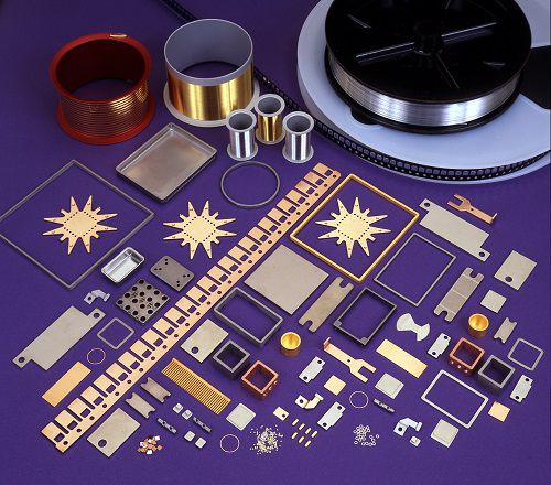
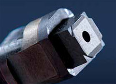
Coining manufactures micro metal stampings that are used as jumper chips, bonding pads, covers, heat sinks, tabs, terminals or other components on microelectronic assemblies and hermetic packages. These precision micro stampings are used primarily to dissipate heat or provide an interface for an electronic circuit or component.
What are Precision Micro Metal Stampings?
Precision micro metal stampings are accurately formed metal components used in microelectronic assemblies to provide electrical, thermal, and mechanical functionality. Manufactured to tight tolerances and consistent thickness, they enable reliable integration into fine‑pitch and high‑density electronic packages.
They are produced from carefully selected metals and alloys, such as copper, aluminium, molybdenum, tungsten, and Kovar™, with optional plating or cladding to improve solderability, corrosion resistance, and assembly efficiency. Their controlled geometry and material properties support improved heat dissipation, electrical performance, and assembly repeatability in demanding, high-reliability applications.
Key Features of Micro Metal Stampings
- Custom developed micro stampings in dimensions as small as 100µm (0.004″)
- Ability to create precision stampings from a variety of metals
- Most common are aluminium, copper, Molybdenum & Kovar
- Optional plating – Ni, Au, Ag
- Cladding service also available: metal to metal & solder to metal
Precision Metal Stampings Resources
Coining Microstampings Brochure
Bond Pads Brochure
Bio-Implantable Composite Materials
Coining Cover Assemblies Brochure
Copper Clips Brochure
Coining Company Brochure
Micro Metal Stamping Materials
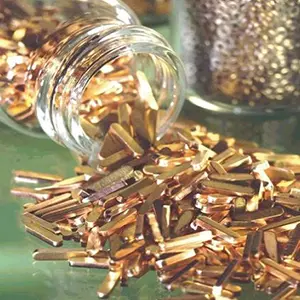
The micro stamped parts, are available in a range of materials, including Kovar™, Molybdenum, tungsten, copper, aluminium and various other metallic compounds, commonly found in metal and ceramic microelectronic packages. Some of these parts are supplied after nickel plating or gold plating
- Materials: Kovar™, Molybdenum, Tungsten, Copper, Invar, and clad metals.
- Applications: RF/microwave packages, implantable medical devices, photonics, and power electronics.
- Capabilities: Coining’s micro-stamping processes support complex geometries and ultra-fine tolerances, with tooling libraries that reduce setup costs and lead times.
Coining Stampings and Materials
Other Coining stampings are manufactured from clad strip consisting of two or more metal layers bonded together in a specialty rolling operation, also called metallic bonding. Two thin layers of strip are run through a roll-compacting mill that bond the two layers of metal together. Solder can then be clad to one or both sides of this strip, allowing customers to minimise the number of placement operations in semiconductor assembly.
Coining utilises its own in-house tooling department to review, design and build tooling to customer specifications. They also use progressive dies to create a variety of 3 dimensional configurations, or EDM-built tools to provide extraordinary precision and variety to the geometries of their parts. Coining primarily focuses on two-dimensional micro-stampings with constant cross-sectional thicknesses less than 0.75mm (0.030″).
Coining also offers a range of Bio-implantable Composite Materials, or BCMs. These are used in critical applications such as cardiac rhythm management, neuromodulation, defibrillators, urology, prostate cancer treatment, and charging antennas. These BCMs include metals such as Titanium, Niobium, copper, nickel & gold. They remove the need to replace batteries in implantable devices, and resolve the issue of premature device failure by allowing longer lasting charge.
Key Characteristics of Precision Micro Metal Stampings
- Manufactured to tight dimensional tolerances for consistent performance in fine‑pitch and high‑density microelectronic assemblies
- Used to provide electrical interconnection, thermal management, or mechanical interfaces within electronic packages
- Produced from a wide range of metals and alloys, with optional plating or metal‑to‑metal and solder cladding for enhanced functionality
- Widely applied in semiconductor packaging, aerospace and defence electronics, photonics, RF and microwave devices, and other high‑reliability systems
Got a Question About Precision Micro Metal Stampings?
Whether you’re developing a new product or refining an existing process, Inseto’s team of experts is here to help.
From selecting the right micro metal stamping to optimising your processes, we provide technical guidance, documentation, samples and on-site training to support your application needs.
Knowledge Base Articles
Related Products




Further Information
Wiki – Integrated Circuit Packaging
Applications
Die Bonding, Material Interconnect, Heat Dissipation, Thermal Interface, Package Construction & Sealing, Attaching, Soldering etc.
Industry Segments
Semiconductor Production, Military & Aerospace, Telecommunications, Medical Electronics, Photonics Components, Microwave Electronics, Microelectronics, Power Semiconductor Assembly, Semiconductor Back-end Assembly, PCB Assembly Industries, Universities, Passive Component Manufacturing, Medical Devices
Coining Website
Region
Available from Inseto in the United Kingdom, Ireland & Nordic Region
Request Form
 Back to top