
Wafer Scribing and Contact Angle Measuring Instruments by OEG
OEG GmbH, founded in 1991 develop and manufacture a range high-precision contact angle measuring equipment and precision wafer scribing systems for industrial and research applications in the semiconductor and optics industries etc. OEG has delivered and installed hundreds of machines worldwide, with customers now on every continent.
Producing a wide range of standard products, based on more than 30 years experience, OEG’s instruments include precision manual wafer scribing systems, contact angle and surface tension measuring equipment for manual or automatic sample processing, including:
“MR 200” Precision micro diamond scriber for precise manual scribing on semiconductor wafers and related substrates up to 200mm in diameter.
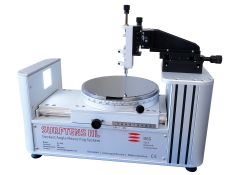
“SURFTENS HL” meet the needs for a fast, highly accurate and comfortable measurement of the wettability of silicon wafers up to 200mm in diameter.
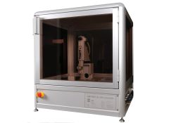
“SURFTENS HL automatic” a 300mm diameter single wafer tool designed for use in semiconductor industry and research, in particular for process control of wafer coatings and in the photolithographic process.
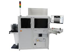
“SURFTENS WH 300” suitable for any cleanroom class, the system features automatic mapping of wafer contact angles and is equipped with a 3 axis wafer robot, wafer scanner, load-port for 200 and/or 300 mm wafers, fan filter unit, SECS/GEM Interface and notching system.
Other products include “SURFTENS Basic“, a low cost contact angle meter that provides all functions for measurement of contact angle and surface free energy and “SURFTENS UNIVERSAL“, a reliable measuring instrument for contact angle, surface free energy and surface tension with many options like motorized dispenser, multi dispenser and tilting stage.
MR 200 Wafer Scriber
Wafer scriber for scribing pieces up to 200mm wafers, ideal for research or development applications.

More
SURFTENS HL
Manual Contact Wafer Angle Goniometer suitable for measuring up to 200mm wafers.
More
SURFTENS HL Automatic
Automatic single wafer Contact Angle Goniometer suitable for measuring up to 300mm wafers.
More
SURFTENS WH
Fully automatic contact angle and surface tension tool with micro scriber for up to 300mm wafers.
More
Further Information
Contact Angle Measurements in Semiconductor Fabrication
Contact angle measurement is a technique used to quantify the wettability of a surface by observing the angle formed between a liquid droplet and the solid surface. In semiconductor fabrication, this measurement is critical for assessing surface energy and cleanliness, which directly impact adhesion, coating uniformity, and process reliability.
Benefits of performing contact angle measurements on semiconductor wafers:
- Surface Quality Control: Small changes in wafer surface properties significantly affect adhesion of photoresists and coatings. Contact angle measurements quickly reveal these changes, enabling process optimisation.
- Improved Yield: By ensuring proper wettability, manufacturers reduce defects such as voids or uneven coatings, improving device performance and reliability.
- Non-Destructive & Fast: Measurements are quick and do not damage wafers, so can be used to sample or to continuous monitor processes.
- Enhanced Cleaning Efficiency: Hydrophilic surfaces (low contact angle) allow better interaction with cleaning solutions, ensuring contaminant removal before critical steps like lithography or bonding.
Wiki – Semiconductor Device Fabrication
Applications
Semiconductor Wafer Research, Semiconductor Wafer Fabrication, Contact Angle Measurement, Wafer Scribing
Industry Segments
Semiconductor Fabrication, Photonics, Bio Medical, Consumer Electronics, Aerospace, Defence
OEG Website
Region
United Kingdom, Ireland & Scandinavia/Nordic Regions: Finland, Sweden, Norway & Denmark
Request Form
 Back to top