Andover, United Kingdom – Lincoln-based RF and microwave design consultancy Cogent RFMW enhances its semiconductor verification and characterisation services through the use of a SemiProbe probe station, supplied by Inseto.
SemiProbe Probe Station Testing High-Frequency Devices at Cogent RFMW
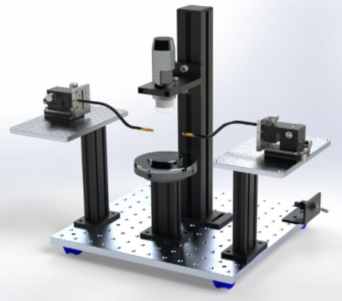
Inseto, a leading technical distributor of equipment and materials, has supplied a SemiProbe probe station to RF and microwave design consultancy Cogent RFMW, enabling the company to enhance and extend its semiconductor verification and characterisation services.
Used in conjunction with benchtop T&M instrumentation, the probe station is being used for DC tests – including pulsed and continuous IV curves, Gummel plots, breakdown voltages and current gain – and RF tests that include small and large signal S-parameters, noise figure and load-pull linearity. All tests can be performed on wafers or die.
“The semiconductor industry is changing in the UK, and skills shortages are making it difficult for many manufacturers to do everything in house, even if they have the equipment,” comments Malik Ehsan Ejaz, Founder and CTO of Cogent RFMW. “At Cogent we have much sought-after skills, and the SemiProbe station supplied by Inseto plus equipment from Interligent and Focus Microwave enable us to support UK-based IC OEMs.
Ejaz, formerly Principal Engineer at CSA Catapult, goes on to say that skills shortages are the biggest hurdle manufacturers face.
Matt Brown, Managing Director of Inseto, adds. “The supply chain has had to re-invent itself in recent years to bring real value to customers. For instance, in 2021 we established a Process Development Laboratory, which is now in almost constant use, plus we’ve introduced equipment operation training courses. What Cogent RFMW is doing is another great example of how the industry is changing. A consultancy that is fully hands-on with advanced equipment and has the expertise to support semiconductor OEMs.”
Based in Lincoln, Cogent RFMW is well positioned to serve semiconductor manufacturers in the Midlands and the North.
Inseto is exclusive distributor for SemiProbe in UK, Ireland and Northern Europe.
E-Mobility Technology International Publication – Read all about the process development of “Wire Bonded” battery connections in the Summer 2022 edition.
For any type of vehicle, or electrotechnical machine for that matter, in which the drivetrain is largely electric, the battery is its defining component. It determines performance. Also, the reliability of the battery pack is a major contributor to the overall reliability of the EV or machine. There is also the cost aspect. In the case of an EV, the battery pack accounts for almost one-third of the vehicle’s cost. And over a third of the cost of the battery pack is in its manufacture.
Understandably, battery pack manufacturers are seeking to get the most from well-established and proven manufacturing technologies to make increasingly dense and complex battery packs, while assuring high reliability and keeping costs as low possible.
As readers will be aware, a battery pack comprises several battery modules that are connected (using bars, bolts or heavy gauge cables) in parallel and series combinations to produce the desired energy and power characteristics. Each module contains several cells – of pouch, prismatic metal can or (most commonly) cylindrical type – connected to a busbar.
The two most popular methods for connecting cells to busbars are:
Laser welding. Each busbar (typically a complex shape) is placed in physical contact with the respective terminals of all cells to which it is to be connected. The contacting surfaces are then fused with a weld.
Ultrasonic wirebonding. This is an ambient temperature ‘friction weld’ process. The controlling variables that determine the process are the ultrasonic energy, the bonding force applied by the wedge and the bond cycle time.
Both methods have clear benefits. And both have some limitations. For instance, laser welding is non-contact, and the beam can be projected into spaces that cannot necessarily be accessed by a wedge bonder. On the downside, tooling can be an issue to account for any cell height tolerances. Also, as it is a traditional weld process, there’s a risk of localised heat from the welding process penetrating the negative terminal and damaging the cell. Note, a cylindrical cell’s positive terminal is ‘floating’, so less vulnerable to heat transfer because of an air gap.
As for ultrasonic bonding (see figure 1), it is an ambient temperature process (that can be used to place wire or ribbon) so there is minimal localised heating and no risk of damaging cells. Also, the process copes far better with tolerances in cell height (relative to the busbar) and, when wire is used, by matching its cross-sectional area and length to a maximum desired current each cell is effectively given its own in-line fuse.
This is a great safety feature, as a shorting cell will self-isolate and protect the module. However, due to the application of ultrasonic energy in the wirebonding process, all components (e.g. cells, busbar etc.) must be clamped sufficiently to ensure no harmonic resonance can occur to compromise bond integrity.
Finite element analysis reveals where best to attach wire bonded connections to battery cells
While there are many ‘laser weld versus wirebonding’ debates taking place in the industry, both techniques have their respective places; and industry bodies, equipment OEMs and distributors alike are working closely to help battery pack manufacturers identify, develop and optimise the best processes for their applications.
For instance, where wirebonding is concerned, wedge bonder OEM Kulicke & Soffa (K&S) offers ultrasonic modelling (see figure 2) to identify the exact bonding responses expected from the unsupported end cap, eliminating the need for customers to invest in complex tooling and fixtures.
Industrialisation
The challenges associated with battery module welding (including wirebonding) were explored in a presentation delivered by the UK Battery Industrialisation Centre (UKBIC) at the Battery Test Expo at Silverstone, United Kingdom, in May 2022. Based in Coventry, UKBIC is a 20,000m2 manufacturing research facility. It is used for the trialling of new materials, cell formats, module and pack structures, and manufacturing processes.
UKBIC’s presentation highlighted that, to achieve high consistency and yield in welding battery modules, cells and modules must be designed to be more work-friendly for the welding process (irrespective of which type) in terms of their geometries and choice of materials.
Also highlighted were challenges associated with investment costs, access to equipment, knowledge and skills. Regarding these, OEMs and the supply chain are stepping up to the plate. As mentioned, K&S offers ultrasonic modelling to help customers develop their processes. Also, Inseto (which is supporting UKBIC through partnership with the supply of a K&S Asterion EV hybrid wedge bonder) has invested in its own wedge bonder for use in a process development laboratory. Both the investment and provision of a laboratory for customers to use are not standard practice for a distributor. Nor is bonder use training. Something else Inseto offers.
Several battery pack manufacturers have already used the laboratory to develop and optimise their processes, establishing the ideal mix of wire gauge and bonder control parameters. They have also been exploring how to handle surface contamination, as the cleanliness and plating quality of commercial cylindrical cells often used for battery packs can be problematic, irrespective of weld method. As the battery cells are live during assembly (typically 30% charged), the cleaning process must not short the cells or impact the internal battery chemistry.
Similarly, UKBIC is focused on support – and more than just technical. For instance, the centre aims to help manufacturers rise to other challenges, such as helping manufacturers create safety policies – as many policy makers may not be fully aware of the safety regulations associated with battery manufacturing. Procedures will need to be in place for transportation, storage and handling.
In summary, these are exciting times for the e-mobility sector and whilst there are many challenges ahead it’s encouraging to see how industry bodies, OEMs and distributors are rising to these.
Andover, United Kingdom – Inseto, a leading technical distributor of equipment and materials, has supplied and installed a Kulicke & Soffa (K&S) Asterion EV hybrid wedge bonder at the UK Battery Industrialisation Centre (UKBIC).
The UK Battery Industrialisation Centre (UKBIC) offers and develops wirebonding using a K&S Asterion EV wedge bonder, supplied and installed by Inseto.
The Asterion EV gives the national battery manufacturing development facility, UKBIC, the ability to provide a wider range of welding technologies to its customers. The new bonder – specially created to support battery module manufacturing – complements the facility’s existing laser welding capability, meaning the facility can now offer different welding technologies dependent on the application.
Andrew Britton, UKBIC’s Business Development Manager, said: “We’re delighted to be collaborating with Inseto on the installation of this new bonder at UKBIC, meaning that we can offer more welding choice to our customers. The bonder also features a non-destructive inline pull test capability to check weld quality. Also, with wirebonding, cells can be reworked and recycled more easily at end of life.”
Matt Brown, Managing Director of Inseto, added: “We’re delighted to be collaborating with UKBIC so that they can offer wirebonding as a means of interconnecting the many cells in a battery pack. Laser welding and ultrasonic wirebonding processes both have roles to play in battery pack manufacturing, but it’s the latter’s ability to place suitably sized wires that can act as individual fuses for each and every cell that’s got people interested. Also, there’s no need to pre-form complex busbars, which is the case for laser welding.”
The K&S Asterion EV, one of the most advanced bonders in the battery sector, is ultrasonic and uses ambient temperature ‘friction welding.’ It can place and bond aluminium wire in the 100 to 600µm diameter range and copper wire in the 100 to 500µm diameter range.
MAIN ENDS
About UKBIC
The £130 million UK Battery Industrialisation Centre (UKBIC) battery manufacturing development centre was opened by the Prime Minister in July 2021. The unique national facility provides the missing link between battery technology, which has proved promising at laboratory or prototype scale, and successful mass production. Based in Coventry, UKBIC welcomes manufacturers, entrepreneurs, researchers and educators, and can be accessed by any organisation with existing or new battery technology – if that technology brings green jobs and prosperity to the UK.
In addition to funding from the Faraday Battery Challenge through UK Research and Innovation, UKBIC is part-funded through the West Midlands Combined Authority. The facility was delivered through a consortium of Coventry City Council, Coventry and Warwickshire Local Enterprise Partnership and WMG, at the University of Warwick, following a competition in 2018 led by the Advanced Propulsion Centre with support from Innovate UK.
POWERING UP – Boundaries are being pushed in all engineering sectors, but few more so than with regards to power electronics. Matt Brown, Managing Director of Inseto and Andy Longford, Technical Consultant at PandA Europe explain.
For every problem solved in the power semiconductor industry, it seems that at least one other is introduced. Where performance is concerned, the goals are typically to increase power density and to operate at higher switching frequencies. These goals have been met by moving from silicon (Si) to wide bandgap materials, and silicon carbide (SiC) has become extremely popular.
To date, only relatively simple structures such as diodes and mosfets have been fabricated in SiC and are commercially available. These tend to be in standard packaging and that is what limits their operating temperature range. However, many applications are calling for more advanced structures and/or the ability to cope with higher temperatures.
In theory, any semiconductor device structure that can be fabricated in Si can, with suitably adjusted manufacturing processes, be made in SiC and a far higher (5x to 10x) power density should be achievable. Tests are necessary to confirm that theory can be put into practice. The University of Warwick, for example, has a dedicated Power Electronics Applications and Technology in Energy Research (PEATER) group for research into SiC power electronics and the development of fabrication processes for bipolar SiC power semiconductor devices. Expertise covers fundamental materials research, device simulation and optimisation, fabrication, characterisation, packaging and reliability testing.
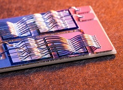
Semiconductor Device, image courtesy of University of Warwick
It is worth noting that thermal cycling is an important factor. For example, AEC-Q100, the qualification test for packaged integrated circuits for automotive applications, details four ambient operating temperature ranges. The widest range is -40oC to 150oC. But SiC-based devices will, subject to packaging, be able to operate at far higher temperatures. It is not hard to imagine a SiC die at the heart of an automotive component in a vehicle working in a cold environment cycling from sub-zero temperatures to more than 300oC several times a day.
As part of its work with the EPSRC (Engineering and Physical Sciences Research Council) Centre for Power Electronics, the university has already produced SiC insulated-gate bipolar transistors (IGBTs) with breakdown voltages of 10kV, noting that silicon IGBTs are typically rated up to about 5kV. In addition, full gate control has demonstrated the viability of the technology for applications including high voltage DC transmission.
Testing and characterisation are performed using a SemiProbe PS4L probe system and other equipment in the university’s dedicated wide bandgap semiconductor characterisation facility. Thanks to a degree of automation, the tests are highly repeatable and are producing a wealth of data. This means that for any given manufacturing process and desired device performance goals it is possible to determine the yield from a SiC wafer.
Make the connection
To benefit from a SiC semiconductor die’s ability to operate at a high temperature – noting that SiC power semiconductors can operate with junction temperatures in excess of 500oC – it is best to attach it to a substrate, such as copper, which will provide good heat dissipation. However, solder cannot be used because it has a melting point lower than the kind of temperatures the SiC die might reach. For example, the popular lead-free SAC alloy (96.5% Sn, 3% Ag and 0.5% Cu) melts at about 230oC. Also, at only a few tens of Watts per meter-Kelvin (W/(m.K)), solder is not that good a thermal conductor.
An alternative to soldering is sintering, a manufacturing process that is a combination of heat and pressure. Silver is currently the most popular sintering material. Its melting point is about 960oC and the thermal conductivity of a sinter paste is very good (between 130 and 250W/(m.K)).
Silicon Carbide Die attached using Silver Sintering
The sintering process is as follows. A sinter paste comprising monometallic particles, of less than 1μm in size, and a resin are printed (in a similar way to solder paste) onto a substrate in patterns corresponding to the shapes and locations of the SiC dies. The substrate is heated to evaporate the resin and the dies are placed. Pressure, which can be up to a few tens of MPa, is applied as a downwards force. It serves two purposes. First, a lower temperature can be used to bond the materials, yet the bonds achieved will be able to operate at a higher temperature in the field. Second, it reduces the risk of voids, which can lead to delaminating and cracking over time. Note: checking for the presence of voids requires the use of a scanning acoustic microscope as x-ray equipment does not work; the power required to penetrate the metallic substrate is so high it makes the die virtually invisible.
Sintering for die attach is a relatively new technology. For example, the North East’s Driving the Electric Revolution Industrialisation Centre (DER-IC) – funded by UK Research and Innovation and set up in 2020 – has just taken delivery of an AMX P100 sinter press. It employs a Micro-Punch system that allows equal force to be applied to multiple dies of varying thickness. Compared to using a single (flat) punch, this mitigates against the risk of voids forming beneath thinner dies.
DER-IC will provide open access facilities and aims to bring together the UK’s technology and manufacturing expertise in electrification research and development. It is believed DER-IC is the first facility in the UK to take delivery of a sinter press as advanced as the AMX P100.
Supply chain
In many cases, those developing next generation SiC-based power devices are in unknown territory. They have volume (space) and ideal performance characteristics in mind, but can such a device be made?
Few organisations will want to invest in cap-ex equipment, which is why the services offered by the North East’s DER-IC have such an important role to play. The Compound Semiconductor Applications Catapult, a DER-IC for the Southwest and Wales, offers services too. Its Power Electronics Laboratory is heralded as one of the country’s most advanced and comprehensive modelling, characterisation, integration and validation facilities for power electronics innovation. It also provides advanced packaging capabilities for power electronics.
Distributors are doing their part too. For instance, Inseto has a Process Development Laboratory at its headquarters in Andover. In 2021, the company invested in a Kulicke & Soffa Asterion wedge bonder to join its materials test and plasma cleaning equipment. A major OEM of power ICs is, at the time of writing, using the facility. Also, several companies have been using the facility recently to develop battery cell wirebonding processes. These companies range from existing battery pack manufacturers exploring new processes to start-ups doing prototype runs. In all cases they have access to equipment they cannot yet afford to invest in.
That, plus access to expertise.
Empowered
In summary, the production of next generation power semiconductor devices requires new types of equipment and processes. But that is to be expected considering the use of materials such as SiC. What is interesting is the amazing level of collaboration between industry and academia, and roles being played by OEMs and distributors to de-risk programmes. Engineers have access to expertise that is confirming if custom (and potentially high volume) power devices can be fabricated. And if so, how.
Inseto is proud to reproduce the above article first published in Electronics Weekly on 27th April 2022, with the kind permission of the editor.
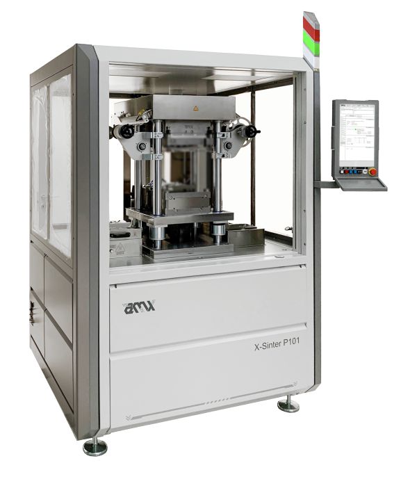
DER-IC North East is the first facility in the UK to install an AMX P100 die attach sintering press with micro-punch capability for the manufacture of power semiconductor components. (Image courtesy of AMX Automatrix.)
Andover, United Kingdom – Inseto, a leading technical distributor of equipment and materials, has supplied Driving the Electric Revolution Industrialisation Centre (DER-IC) North East with equipment to enhance its power electronics, machines and drives (PEMD) capabilities. Of the equipment supplied, an AMX P100 die attach sinter press is the first micro-punch machine to be installed in the UK and will enable the manufacture of high-reliability high-power modules.
Sintering is a manufacturing process that combines pressure (mechanical force) and temperature to bond materials using a sinter paste. The process is increasingly required for the packaging of high-power semiconductor modules that incorporate silicon carbide (SiC) dies which, when channeling high currents, can produce heat at temperatures far higher than the melting point of solder (as traditionally used for conductive die-attach).
As for the AMX P100’s ‘micro-punch’ capability, this relates to how most sinter presses use a flat, single punch to apply force to the top of the dies. But if the dies are of different thicknesses, the same force cannot be applied across all. This means there is a risk of voids forming in the sinter paste beneath thinner dies – which in turn can result in failures in the field because of the high voltages and currents being switched. The AMX P100 can apply equal force to all dies, irrespective of their thickness.
Professor Derrick Holliday, Technical Director for DER-IC North East comments: “The drive by industry to create highly efficient, power dense and integrated power converters places increasing demands on power semiconductor switching devices. Manufacturers must be confident that products operating under these demanding conditions, particularly in safety-critical applications, are reliable. By ensuring the highest integrity bonds, this advanced die attach sintering technology will facilitate the development of novel and advanced semiconductor packages and converter topologies, as well as supporting broader power switching device research, by both industry and academia.”
Inseto has also supplied DER-IC North East with two other pieces of equipment that will be used within the new facility for the manufacture of power modules and packs, as well as other components needed for PEMD.
The first machine is a Kulicke & Soffa Asterion hybrid wedge bonder. Features include an expanded bond area, robust pattern recognition capabilities and extremely tight process controls. Together, these features deliver heightened productivity, bonding quality and reliability.
The second machine is an Amadyne FAB1 (flexible automatic die bonder). It is a modular micro assembly production platform designed for complex high mix and high-quality products. Features include short setup times (i.e. fast product changeovers, ideal for prototyping and process development) and remote system support / diagnostics.
Rachel Chambers, DER-IC North East Chief Operating Officer, comments: “It’s critical for us to ensure we provide best-in-class equipment and capabilities to support companies on developing, prototyping and scaling up their manufacturing processes. The sintering equipment in particular will give those using our facilities accesses to advanced manufacturing capabilities, and my team and I are looking forward to working closely with Inseto in helping all users meet their PEMD goals.”
DER-IC North East’s new die attach sintering press is a ‘micro-punch’ system that can apply equal pressure to the top surfaces of dies of varying thicknesses, thus reducing the risk of voids forming beneath the thinner dies. (Image courtesy of AMX Automatrix.)
Andover, United Kingdom – SemiProbe has introduced a new family of small-footprint, low cost probe station for basic characterization for small sample testing of samples from die up to 100mm diameter.
SemiProbe mini-PS4L Low Cost Probe Station – Manual Version
The new “mini-PS4L” low cost probe stations are available in either manual or semiautomatic configurations to address multiple applications and testing requirements on devices that are 100 mm or less in size.
Developed in response to market requests for smaller footprint lower cost solutions for basic characterization of small samples, the systems feature a wide-range of modular accessories including DC or HF versions for testing partial or full wafers, individual die or packaged parts etc.
The mini-PS4L series is an expansion of the popular and patented Probe System for Life (PS4L) systems that address an even wider variety of wafer sizes and applications. The PS4L system is the most modular on the market and provides a perpetual field upgrade path. A unique “mini-PS4L” proposition offered by SemiProbe, is a full credit (conditions apply) if customers upgrade to the larger PS4L system.
Inseto is exclusive distributor for SemiProbe in UK, Ireland and Northern Europe.
Andover, United Kingdom – Inseto Invests in Wedge Bonder for its Process Development Laboratory and Launches Two Bonder Operation Training Courses
Kulicke & Soffa Asterion Wedge Bonder Installed at Inseto’s new “Process Development Laboratory”
Inseto, a leading technical distributor of equipment and materials, has invested in a Kulicke & Soffa (K&S) Asterion wedge bonder. Located in Inseto’s new Process Development Laboratory along with materials test and plasma cleaning equipment, the automatic bonder is suitable for the large-wire, fine-wire and ribbon bonding of hybrid circuits, semiconductor devices, sensors, and automotive power modules and battery packs.
Inseto has also launched two training courses: one for wedge bonding, the other for ribbon bonding. Both are delivered by Inseto’s factory trained and highly experienced engineers. Course content is tailored to meet a trainee’s exact requirements and modules include bond theory, bonding tool and wire/ribbon selection, machine setup and operation, process development and bond quality control, and maintenance and repair.
Matt Brown, Inseto’s Managing Director, comments: “These are challenging times for manufacturers. To take full advantage of industry’s latest manufacturing techniques companies must first develop and optimise their processes. They then need to ensure they’re getting the most from their equipment when they move into volume production. Early access to best-in-class equipment and thorough training for operators are therefore essential.”
Brown goes on say that most equipment distributors simply carry demo machines – on loan from their suppliers and which they intend to sell. Inseto, on the other hand, is investing in kitting out its own Process Development Laboratory.
“While all distributors say they’re committed to supporting their customers, we’re demonstrating our commitment through investment,” continues Brown. “Our laboratory is a quiet environment that doesn’t have distractions you find in a manufacturing environment. And with our specialists to hand it’s the ideal place to build and evaluate prototypes, and to receive training.” Inseto’s Process Development Laboratory is fully operational. Also, the company is now taking bookings for its bonder operation training courses, which can be delivered on customer premises if required.
When applied to a wafer, an oxide coating adds a dielectric or passivation layer, needed to give a semiconductor, MEMS or BioMEMS device its desired electrical properties.
In our “Oxide wafer coatings: their properties and application methods” article, we discuss the two most common oxidation processes – Atmospheric Thermal Oxide (ATOx) and Plasma Enhanced Chemical Vapour Deposition (PECVD) – and provide examples of applications that benefit from both.
We discuss oxide growth rate, and how it is influenced by temperature, the presence of other chemicals (water/steam in the case of wet ATOx), doping and crystal orientation.
Also, did you know, that during the oxidation process, oxide grows into the wafer as well as onto its surface. For silicon, the ratio is about 46% into the surface and 54% on top of the original surface. In other words, the overall wafer thickness does not increase by the depth of the oxide layer, as some of the Si is consumed during the oxidation process.
Inseto produces and supplies an extensive range of high-quality oxide coated semiconductor wafers used for production and research purposes.
Inseto will be showcasing DELO’s range of adhesives at the Battery Tech Expo and Battery Technology Show this October.
Adhesives for Battery Pack Assembly
Andover, United Kingdom – Used extensively in #EV #batterypacks, #adhesives play important roles. Here are just a few examples of what they are used for and the properties the adhesives must possess.
In carriers (pictured), adhesives are used for the bonding of cylindrical cells. Also, retainer bars are bonded onto the cells plus the carrier is bonded to a busbar. The adhesives also provide vibration protection and, hand in hand with that, help reduce noise.
The adhesives must also be flame retardant and bond to flame retardant materials. The coefficient of thermal expansion (CTE) needs to be close to that of the other materials, and curing time needs to be short for volume production scenarios.
Adhesives are also used for weld and pin sealing in #batterymodules and #powerpacks and provide corrosion protection. The power management electronics used in packs also use adhesives; for die-attach and to protect components.
If you’d like to know more, come and talk to us at any of the following shows in October
12th – Battery Tech Expo at Silverstone
19th & 20th – FAST Show (co-locating with EDS) in Coventry (Ricoh Arena)
26th & 27th – Battery Technology Show in Coventry (Ricoh Arena)
Example: Sintering SiC Die Attach of Semiconductor Devices
Check out the our latest “Knowledge Base” article on sintering SiC die first produced for e-mobility technology magazine (Summer Issue #9) and reproduced with kind permission of the editor on our website.
Silicon carbide (SiC) is the semiconductor material of choice for high power semiconductor transistors. They can switch far higher voltages and currents than devices fabricated from silicon. They can also run much hotter, presenting packaging challenges.
A popular substrate on to which SiC die is attached is copper. It is a good conductor of power and heat. However, the thermal conductivity of a typical die attach solder is not great, and melting points max out at circa 220°C.
An alternative to soldering is sintering. A paste comprising monometallic particles and a resin is printed onto a substrate in patterns corresponding to the shapes and locations of the SiC dies. The substrate is heated to evaporate the resin and the dies are placed. The sintering process itself sees a combination of heat and pressure.








 Back to top