
Advanced Packaging Equipment and Services by PacTech
PacTech – Packaging Technologies GmbH is a world leading provider of advanced wafer bumping, packaging and solder ball placement equipment used in numerous applications such as micro BGA, wafer level CSP, Optoelectronic (micro optics, fiber attached and lens alignment), Solder stacking (SS Hard drives), MEMS (2D, 2.5D and 3D packaging) and TSV (solder filling of vias).
PacTech is also a worldwide leader in Wafer Level Bumping & Packaging Services. These services meet the high quality demands of customers and support both engineering and prototyping services, as well as high volume production.
SB² Laser Solder Jetting Systems
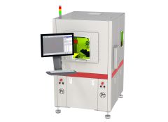
PacTech’s SB² laser solder jetting technology enables precise, contactless solder ball placement at both wafer and device level. Solder balls are placed and reflowed in a single step using a flux‑free laser process, minimising thermal and mechanical stress. SB² platforms are available in manual, semi‑automatic and fully automated configurations, supporting R&D, prototyping and volume manufacturing.
PACLINE™ Electroless Wafer Bumping
The PACLINE™ series provides fully automated, maskless electroless Ni, Pd and Au wafer bumping for reliable under bump metallisation. PACLINE systems support 100 mm to 300 mm wafers and are widely used in WLCSP, flip chip and high‑reliability semiconductor applications.
Laser Assisted Bonding Equipment
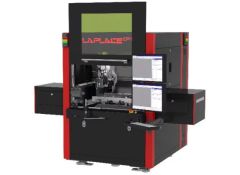
PacTech’s LAPLACE® laser assisted bonding systems provide high accuracy, low thermal stress assembly for advanced semiconductor packaging and electronic assembly. Using localised, selective laser heating, die bonding, placement and reflow are performed in a single step without heating the entire substrate, reducing warpage and protecting temperature‑sensitive devices. LAPLACE platforms support flip chip assembly, wafer level component assembly and fine pitch interconnects across 2D, 2.5D and 3D architectures.
Wafer Level Fabrication and Packaging Services
In addition to equipment supply, PacTech provides subcontract wafer level packaging and solder bumping services through certified manufacturing sites in Europe, the USA and Asia. These services support flip chip, WLCSP, fan‑out wafer level packaging and 2.5D and 3D integration, combining electroless and electroplating, solder balling, laser assisted bonding and wafer level rework.

Laser Solder Jetting Systems
Laser solder bumping equipment, including repair / work of BGA’s.
More
Electroless Bumping Equipment
Fully automatic electroless nickel plating line.

More
Laser Assisted Bonding
Localised, selective laser heating, bonding, placement and reflow.
More
Wafer Level Services
Supporting both engineering and prototyping services.

More
Further Information
What is Wafer Bumping for Advanced Packaging?
Wafer bumping is a critical process in advanced semiconductor packaging that replaces traditional wire bonding with tiny solder or metal “bumps” formed directly on the wafer’s I/O pads before dicing. These bumps create short, highly conductive interconnects between the chip and its substrate, enabling superior electrical performance, lower inductance, and improved thermal management.
By forming these connections at the wafer level, bumping supports high-density layouts and advanced packaging formats such as Flip Chip, Wafer-Level Chip Scale Packaging (WLCSP), and emerging 2.5D/3D integration. The benefits of wafer bumping include:
- Enhanced electrical performance and signal integrity
- Higher current carrying capacity
- Reduced footprint and package thickness
- Compatibility with advanced packaging architectures
Inseto Knowledge Base Document:
Read our guide to “Laser Solder Jetting“
Wiki – Advanced Semiconductor Packaging
Applications
MEMS Packaging, Camera Module Fabrication, Memory, FO WLP, Flip Chip Bumping, BGA Solder Ball Placement, Smart phones and Tablet CSP Packaging, Bio Medical Device Assembly, Sub Contract Wafer Dicing, Sub Contract Wafer Bumping, Sub Contract Solder Bumping
Industry Segments
Semiconductor Fabrication, Photonics, Bio Medical, Consumer Electronics, Aerospace, Defence
PacTech Website
Region
United Kingdom, Ireland & Scandinavia/Nordic Regions: Finland, Sweden, Norway & Denmark, Netherlands, France & Benelux
Request Form
 Back to top