An introduction to Gauge Repeatability & Reproducibility (GR&R) testing on the Dage 4000 Plus / Optima platform (IKB-005).
GRR Testing uses a calibrated weight to perform several lifts using selected load cells. Multiple tests using the same weight verify load cell accuracy and repeatability. If drift / variation are quite large with respect to the selected weight; calibration is recommended.
The weight is dependent on load cell range. For example, WP100 cartridge set to 50g range requires a 50g weight.
Running GR&R Tests:
Data for GR&R on the Plus can be generated from the “Start” – “New Sample” drop down menu or the “New Sample” button on the top bar. (NB: Engineering Access level is needed to perform GRR Testing!)
Select the test group and start “New Sample” from the drop down or top bar button.
Select the (NEW) GR&R tab.
Select the G, R and R test and fill out the jig reference box (if using a shear cartridge).
Set the number of tests required.
Pressing the “Start” button the tests will perform the required number of tests.
Save the Sample
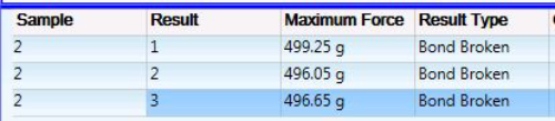
This screenshot shows the GRR Testing Options within “New Sample”.This screenshot shows the final 3 results once testing for GRR is completed.
Matt Houston is a Sales Engineer at Inseto with over 16 years of experience in the microelectronics and semiconductor industry. His background spans process engineering, technical support and technical sales.
He began his career as a Process Engineer at C‑MAC in Great Yarmouth, working on die bonding and wire bonding for high‑reliability, high‑temperature electronic components, opto‑electronics and multi‑chip modules.
At Inseto, Matt has developed broad hands on experience across a range of semiconductor equipment through installations, training and process support. This enables him to support customers in selecting tailored solutions that meet specific technical requirements.
This document advises how to backup and restore the “Dage-Paragon” testing software (IKB-004).
Database Backup Creation
Power up the Dage 4000 Plus platform with the main power switch.
Open the Dage Paragon Software on the PC and initialise the system.
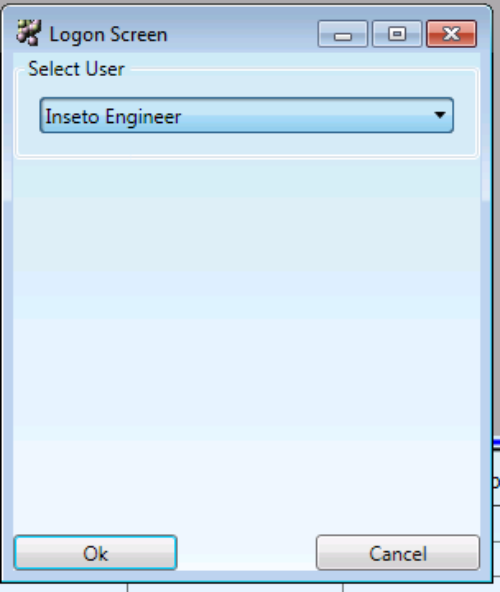
Navigate through the following menus ‘Access / Logon’, and logon with a user account with ‘Engineer Access’.
With ‘Engineer Access’ navigate through ‘Setup / Database’.
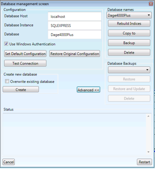
The ‘Database Management Screen’ pop up box will appear, click the advanced button to further open this screen. (This screen can also be opened through Windows start menu ‘Dage Paragon Database Manager ‘)
Select which Database you would like to backup with the ‘Database names’ selection box. (Default is Dage4000Plus).
Click the ‘Backup’ Button.
The ‘Status’ should read ‘Database Backup Finished’ if a successful database backup file has been created.
Click the ‘Restart’ Button to close the ‘Database Management Screen’ and to restart the Paragon software automatically.
Database Restore from Backup
Navigate to the ‘Database Management Screen’ and open the advanced options.
Select which Database file you would like to backup from with the ‘Database Backups’ selection box. (Default is Dage4000Plus).
Click the ‘Restore’ Button.
The ‘Status’ should read ‘Database Restore Finished’ if a successful Database has been created from the Backup file.
Click the Button labelled ‘Save Configuration and Exit’ to restart the Paragon software.
Adam Marshall is a Senior Technical Support Engineer at Inseto Ltd with over 14 years of experience in the semiconductor industry, including 10 years specialising in assembly processes and related equipment. He supports customers across the microelectronics and semiconductor sectors who rely on precision equipment to maintain reliable and repeatable results in production and research environments.
Known for a calm and structured approach, Adam works closely with customers, suppliers and internal teams to deliver clear technical advice and dependable support when it matters.
An introduction to light-activated adhesives, and how to process them (IKB-045).
First there was light-cured adhesives (commonly referred to as “UV adhesives”), then there was light-activated adhesives, and now we have dual-cured adhesives. Of these, light-activated adhesives are the least known and probably the most demanding to work with, in terms of how they are processed, but they offer one significant benefit that the others do not: they can be used to bond non-transparent parts together without using heat as part of the curing mechanism.
“UV adhesives” is the generic term used when referring to an adhesive that requires high-intensity light for curing. A significant proportion of these adhesives actually use light in the visible spectrum (VIS) for curing. A very relevant example is Polycarbonate – most grades of Polycarbonate block UV light (i.e. light that is below 400nm in the electromagnetic spectrum), so a true UV adhesive cannot be used to bond Polycarbonate parts together. Yet there are many instances where “UV adhesives” do work – it is actually the VIS component of the Photoinitiator that is used to achieve the cure!
Regardless of where on the spectrum the Photoinitiator lies, the simple fact is that one of the parts being bonded must be transparent, to allow for 100% cure of the adhesive. No one likes having uncured adhesive in their products on a long-term basis, especially as a number of these adhesives are based on acrylic acid (rendered harmless by curing).
Recent developments in the last 3 – 5 years have resulted in a wide range of dual-curing adhesives that get around this problem. These adhesives, as indicated by the name, contain two curing mechanisms – light (whether UV or VIS), and either humidity or heat. Light and humidity cured adhesives are limited by the fact that the majority of the adhesive in the bond area must be cured by light, and also by the fact that the humidity portion of the adhesive cures at a (slow) rate of 2mm / 24hrs (similar to silicone adhesives), which can be time-consuming.
Light and heat cured adhesives do not suffer from these limitations, however the minimum cure temperature for these adhesives is 80°C, which in effect means setting the oven to ~ 83 – 85°C to avoid any potential cold spots in the oven. This is strongly recommended for this type of adhesive, because if the adhesive does not see 80°C, the heat-cured portion of it will never cure, regardless of how long the bonded parts are in the oven. The time to cure at elevated temperatures can also be a factor, as it can take up to one hour at 80°C. This can be reduced by curing at 150°C for 10 minutes, for example.
For applications where cycle time does not allow for lengthy heat cure stages (even when carried out off-line), or where one of the materials being bonded is sensitive to temperatures even as low as 80°C (as a lot of new, low-cost plastics tend to be), then serious consideration needs to be given to light-activated adhesives.
The theory is simple: dispense the adhesive onto substrate A, illuminate it with high intensity light for a short period of time, place substrate B onto the adhesive, and voila!, the adhesive will eventually be fully cured and the non-transparent substrates will be bonded together with no uncured adhesive in the joint.
In practise, it’s a bit more complicated. The act of illuminating the adhesive with light, called activation, provides enough energy to the adhesive to commence the curing process. If too much energy is provided, there will not be enough time to place the second substrate before a skin forms on the surface of the adhesive. Once this happens, it is then impossible to bond the substrates.
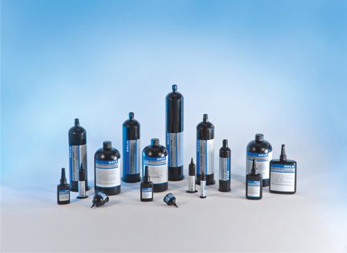
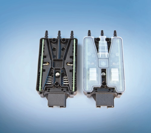
Light Activated DELO-KATIOBOND Example Plastic Bonding Application
The time it takes for the skin to form on the adhesive is called the open time, and is measured from when the illumination ceases to when the skin forms. Increasing the energy provided to the adhesive, whether by increasing the intensity of the light or by illuminating for longer, reduces the open time.
Unfortunately, this is not a linear relationship as other factors such as substrate material, colour, smoothness and reflectivity, all have an impact on the open time. It must be measured for each application, and cannot be transferred across applications. But a very good starting point will be provided in the technical data sheet from the adhesive manufacturer.
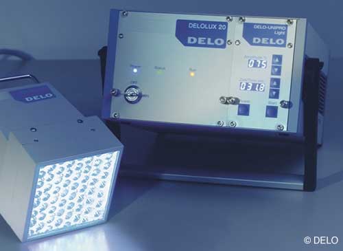
For example, the technical data sheet for DELO KATIOBOND 4594 states that an open time of 15 – 20 seconds results from an illumination time of 3 seconds when using a DELOLUX 400nm LED lamp with a light intensity of 200 mW/cm2, measured at the adhesive. Reducing the activation time will increase the open time, and vice versa. But the extent to which the open time changes will have to be measured! Also, the substrate used was, for standardisation purposes, a piece of waxed cardboard. Changing any of these factors, such as the lamp or the substrate material, affects the open time, which must then be re-measured.
Once the substrates have been joined, full cure will take place over time because 100% of the adhesive has been illuminated prior to joining. If left sitting on a bench, for example, the adhesive will be fully cured 24 hours later, with maximum bond strength. However, this is usually not practical for manufacturing purposes, so accelerating the cure is very often desirable.
There are a couple of ways to do this: first, by adding heat to the assembled parts. This can seem contradictory as light-activated adhesives are used for the very purpose of eliminating heat from the process! But even the addition of low levels of heat can have a significant effect on the cure speed. As a general rule of thumb, for every 10° increase in cure temperature, the cure time is halved (the converse is also true!). So increasing the temperature of the bonded parts to even 45°C can reduce the final cure time to 6 hours, while also ensuring that there is sufficient handling strength in the adhesive to safely carry out the next process on the assembly.
An alternative way to accelerate the cure depends on the geometry of the parts being bonded. If the two parts are identical in X & Y, then this is very difficult to achieve. However, if there is even a slight difference between the parts, for example 0.5mm, then ensuring that a fillet of adhesive is visible around the joint means that a second light cure process can be carried out immediately, significantly increasing the bond strength and allowing the assembly to be moved on to the next process.
Summary
Apply, illuminate, cure – what could be simpler???
Other advantages / tips: Light-activated adhesives are not as reactive as dual-cured adhesives, so frozen storage is not needed. Also, because of this, they can be supplied in larger containers, thereby reducing the cost / gram.
If the substrate on which the adhesive is dispensed is metal, then it will be necessary to heat it up slightly, to say 35°C. This is because the heat that is generated within the adhesive during the activation process will be conducted away from the adhesive by the metal, and so will slow down the reaction significantly, or may even prevent it completely.
For further information on our range of “Light Activated Adhesives”, please click HERE
Eamonn Redmond is a Senior Technical Sales Engineer at Inseto (UK) Ltd, leading the Materials and Adhesives divisions. With nearly four decades of experience in microelectronics, he combines strong technical knowledge with practical commercial insight.
After completing a B.Eng. in Electronics at the University of Limerick, Eamonn began his career at Analog Devices, working as an In‑Line Test Engineer and Process Engineer. During this time, he developed hands‑on expertise in die attach, wire bonding and environmental testing, including burn‑in, temperature cycling and thermal shock. He later progressed to IC Production Manager, gaining experience in wafer‑level and package‑level testing and modern semiconductor production operations.
In the early 1990s, Eamonn moved into technical sales, specialising in die attach adhesives, eutectic solders and materials for wire and ribbon bonding. This role established a strong foundation in adhesive technologies for high‑reliability microelectronic applications.
Since joining Inseto in 1996, Eamonn has supported customers with a wide range of microelectronic materials, including die attach adhesives and encapsulation compounds, alongside substrate materials such as thick‑film inks and thin‑film substrates. He is widely regarded as a key technical resource for customers seeking reliable bonding and encapsulation solutions.
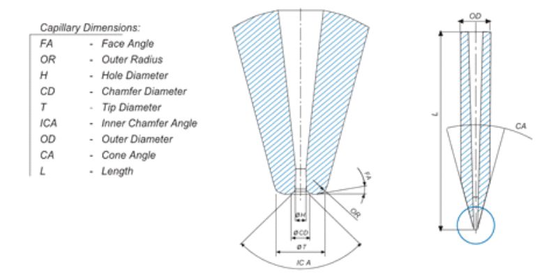
Capillary Nomenclature: Explanation of common features and selection criteria for ball bond capillaries from Kulicke & Soffa, along with the key selection criteria to consider when choosing capillaries (IKB-011).
Capillary selection is key to a successful and stable ball bonding process. Capillaries are high precision manufactured, with attributes specific to the wire diameter in use and bonding process parameters.
Capillaries are manufactured from two main materials:
Toughened Alumina
ATLAS (very high mechanical strength Alumina)
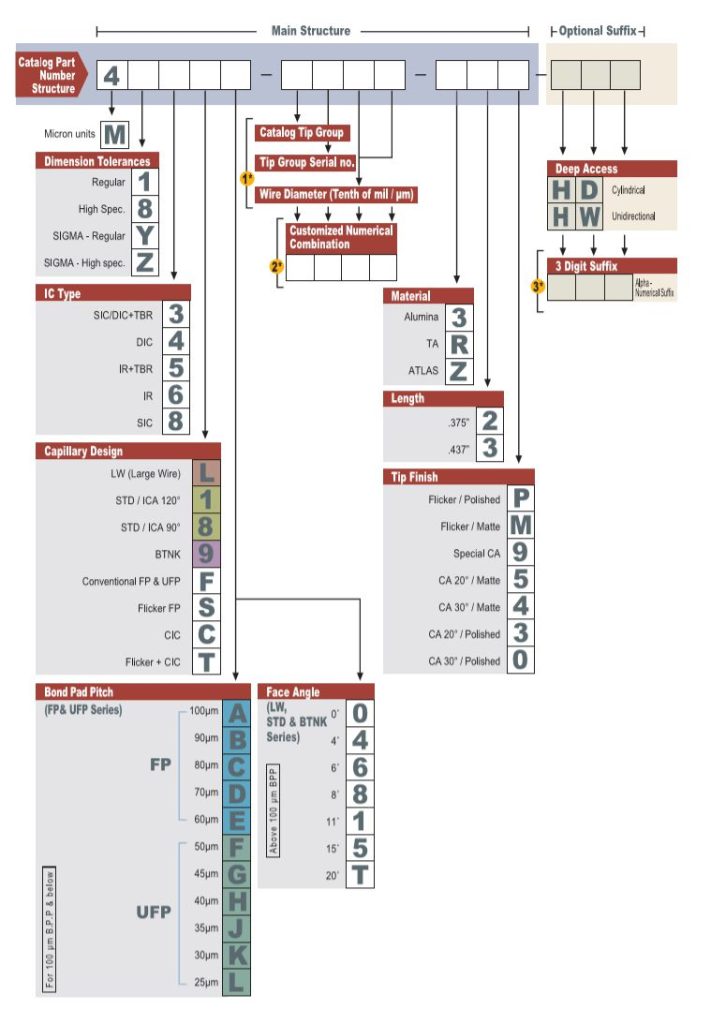
The figure below describes the K&S capillary nomenclature:
There are many factors to consider when selecting the correct capillary. The figure below will show you some of the other considerations that need to be taken into account:
• Hole Diameter (H): This contributes to bond placement accuracy and wire clearance during looping.
• Length (L) This contributes to the need for deeper access in products.
• Outer Radius & Face Angle (OR & FA) This contributes to the formation and finish of the 2nd bond (stitch).
• Inner Chamfer Angle (ICA) This contributes to the housing and formation of the F.A.B (Free Air Ball).
How does laser solder ball jetting technology work?
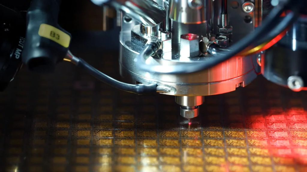
Within the Jetting Head a singulation disc will dispense a single solder ball into the bottom of a capillary where the laser’s thermal energy melts the solder ball, enabling it to shoot under pressurized nitrogen onto any soldering position being reflowed immediately. The process works with various solder alloys, all with different melting temperatures (SnPb, SnAgCu, SnAg, AuSn, InSn, SnBi….), and requires no solder flux. Therefore, laser solder ball jetting is a clean process.
The localised heat and short pulse period of the laser assures that minimal thermal stress is applied to the areas beyond the joined surfaces. The single solder ball dispensing mechanism required no tooling, enabling flexible soldering location and contactless soldering.
The great advantages of this process are the lowered thermal stress of localized heating and no mechanical contact to substrates or delicate components such as MEMS.
The solder jetting process can be used in a number of applications such as discrete devices, probe-cards, memory, camera modules, wafer pieces, PCB, Flex-substrates, BGAs, CSPs, sensors and 3D components like MEMS. Target Markets span Defense, Medical, Automotive and Aerospace.
Specifications:
40µm to 2mm solder spheres.
80µm to 1mm pad pitch.
For further information on our range of equipment for Laser Solder Jetting, please click HERE.
Adam Marshall is a Senior Technical Support Engineer at Inseto Ltd with over 14 years of experience in the semiconductor industry, including 10 years specialising in assembly processes and related equipment. He supports customers across the microelectronics and semiconductor sectors who rely on precision equipment to maintain reliable and repeatable results in production and research environments.
Known for a calm and structured approach, Adam works closely with customers, suppliers and internal teams to deliver clear technical advice and dependable support when it matters.
Chris Valentine appointed to help Inseto’s valued customers further de-risk their semiconductor and MEMS fabrication projects.
Andover, United Kingdom – Inseto, a leading technical distributor of equipment and materials, has appointed Chris Valentine in the role of Technical Sales Engineer to work with customers to de-risk their semiconductor and MEMS manufacturing projects, by advising on material selection and the best tools to use for fabrication and test.
Chris Valentine
Valentine has a Masters in Science (MSci) in Physics from the University of Glasgow and a Masters in Research (MRes) from the University of Cambridge. He is also currently working on a thesis that could result in a PhD in Engineering being awarded by the University of Cambridge. Key subjects studied during his time in academia include advanced carbon nanotube electrodes for electromechanical sensing, MEMs manufacture and photolithography, electrical and nano materials, optical microscopy, solid state physics, semiconductor devices, and nuclear and particle physics.
Matt Brown, Director of Inseto, comments: “We are pleased to welcome Chris onboard. He is set to become a valuable extension to our team of technical specialists, and our customers will benefit greatly from the wealth of knowledge Chris gained during his academic studies and in various research projects.”
Valentine’s PhD research work includes the fabrication of electrochemical sensors to detect chemical analytes; the production of structured carbon nanotube electrodes to control porosity and morphology; and making improvements to the sensitivity and selectivity of fabricated sensors.
Inseto launches comprehensive online store for selecting and ordering silicon, silica, glass, coated and SOI wafers.
Andover, United Kingdom –
– Inseto, a leading technical distributor of equipment and materials, has added an online store to its website for semiconductor wafers. The store, which carries Inseto’s current inventory of wafers, including silicon, silica, glass, coated and silicon on insulator (SOI), features secure online payment and rapid delivery of stocked wafers. Also, Inseto’s online inventory is soon to include sapphire, silicon on sapphire (SoS), lithium niobate, germanium and other materials.
Inseto launches comprehensive online store for selecting and ordering silicon, silica, glass, coated and SOI wafers.
A powerful filtering tool enables users to narrow
down their searches by specifying properties common to all wafers, such as
diameter and thickness. Then, depending on wafer material, the properties
become more specific. For example, silicon wafer properties include ingot
growth method, crystallographic orientation, dopant, grade and upper and lower
surface resistivity.
The site also carries a Semiconductor Wafers Selection Guide. This is accessible from within the online store and from within Inseto’s Knowledge Base, a repository of freely available, viewable and downloadable articles and guides. Brown concludes. “At Inseto, we’re all about customer support. It’s in our DNA. Also, whilst the online store has greatly speeded the wafer selection and ordering process, our experts remain on hand to offer advice and guidance if anyone does have questions.”
Matt Brown, Director of Inseto, comments: “We
have ploughed the combined knowledge of our wafer and supply chain experts into
our online store. In our experience, most customers know the exact
specifications of the wafers they need, certainly in the case of repeat orders,
or they wish to rapidly explore a range of properties and available options.”





 Back to top