Inseto

Month: May 2020

Peel Testing

4th May 2020

What is Peel Testing in materials test and how does it work? (IKB-032)

Peel Testing is a slow perpendicular (usually 90 or 180 degrees) pull that is applied to the work sample with a “peel like” movement involved.

For peel testing, a tweezer pull cartridge is required; once the cartridge has been installed you will be able to select “Peel Test” as a test option. This test is essentially the same as a standard tweezer pull test but with the addition of XY movement in a chosen direction, whilst the tool is applying the upward load.

The image shows a standard peel test, the tweezer jaws close onto the item being tested (top image), the Z axis then moves upwards and the XY stage moves in a specified direction (right image).

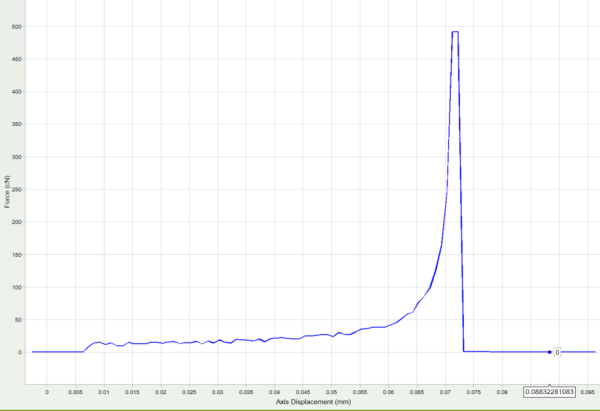
Once a peel test has been carried out and completed then a results graph will be available. The second image shows the force displacement results of a sample peel test performed on a Dage4000Plus Materials Test system.

Essentially anything that needs to have its adhesive strength measured will be peel tested. Examples can include:

  • Adhesive testing; tapes, epoxy etc.
  • Solar panel testing; testing of interconnects, different types of laminates etc…

NOTE: To Perform a Peel test you will require a tweezer pull cartridge and a motorised XY Stage.

Peel Testing Process

Peel test Force vs Displacement Data

Further information:

View more details about the “Tweezer Peel – Pull Test Method“.

View the range of “Nordson-DAGE Bond Testing Equipment“.

Author

Date

Version

Author

Alex Forster

Date

21 April 2020

Version

IKB032 Rev. 1

Download

Atmospheric Plasma Treatment Wand

4th May 2020

What is an Atmospheric Plasma Treatment Wand and what different nozzles are available? (IKB-039)

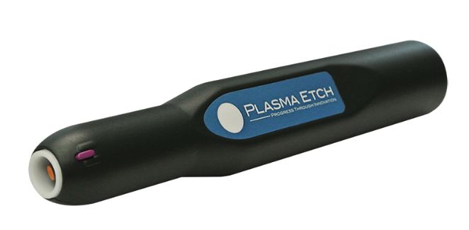
The Atmospheric Plasma Wand is a hand-held device that requires no external gas hook up or vacuum chamber.

Plasma Wands are ideal for spot cleaning and surface modification of large objects before bonding. Applications in microelectronics could include cleaning bond pads prior to wire bonding, or cleaning areas that will be adhesive-bonded.

Surface activation generated with the Plasma Wand lasts about an hour as a rule of thumb, depending on the substrate treated. Metals and silicon last longer than plastics and rubbers.

The Plasma Wand contains three different nozzle selections, what you use will vary depending on your application.

Atmospheric Plasma Wand
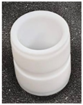
Standard Plasma Wand Nozzle

Standard Nozzle: – This is used for cleaning plastic, rubber and non-conductive materials.

Nearfield Nozzle

Near Field Nozzle: This is used for cleaning metal and conductive materials. It works by creating secondary plasma between the glass and any surface that conducts electricity. It needs to be within 4mm of the surface to create this secondary plasma and it will be visible to the unaided eye. This nozzle will not work on surfaces that do not conduct electricity.

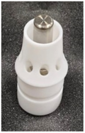
Multi Gas Nozzle

Multi Gas Nozzle: Using the supplied 2mm ID hose, it is possible to introduce a non-flammable input gas to create secondary plasma. The multi-gas nozzle may be used on metal surfaces if you are using argon or helium. It may not be used on metal with room air or any other gas.

For more information on Plasma Etch, atmospheric cleaning equipment, please click HERE.

Author

Date

Version

Author

Matt Houston

Date

28 April 2020

Version

IKB039 Rev. 1

Download

Author Biography

Matt Houston is a Sales Engineer at Inseto with over 16 years of experience in the microelectronics and semiconductor industry. His background spans process engineering, technical support and technical sales.

He began his career as a Process Engineer at C‑MAC in Great Yarmouth, working on die bonding and wire bonding for high‑reliability, high‑temperature electronic components, opto‑electronics and multi‑chip modules.

At Inseto, Matt has developed broad hands on experience across a range of semiconductor equipment through installations, training and process support. This enables him to support customers in selecting tailored solutions that meet specific technical requirements.

What is Imprint Lithography

4th May 2020

This document provides an overview of Micro and Nano Imprint Lithography (IKB-054).

What is Imprint Lithography?

Imprint lithography is a key technology for many emerging applications such as micro-optics, augmented reality, MEMS and optoelectronic sensors; but what is it and how does it work?

Photolithography, be that optical, electron-beam or imprint, is the process of transferring a pattern from one object onto another. Electron-beam and optical photolithography are used to transfer a two-dimensional pattern either from a photomask or a computer program onto a substrate. Imprint lithography is concerned with the transfer of three-dimensional patterns and structures to a substrate.

A typical imprint lithography process consists of the following steps:

  • The wafer is coated with an imprint resist and aligned with a stamp
  • The wafer and stamp are brought into contact and the resist fills the cavities in the stamp.
  • The resist is solidified through UV cross linking or an external thermal source
  • The stamp is removed and the resist is left imprinted with the desired pattern
Imprint Lithography Process
Imprint Photolithography Process

Crucial to the imprint process, is the fidelity of the stamp containing the 3D pattern. Typically, this design will have submicron features that need to be reproduced to a high tolerance. The process for producing these master stamps can be lengthy and expensive, so precise control of the imprint and removal are required to ensure no damage to the stamp. Often, to protect the master copy of the pattern, the stamp used in day-to-day fabrication is an imprinted replica. This stamp will do many hundreds of imprints before it must be replaced, as the integrity of the surface slowly degrades and the yield of the devices produced decreases.

The limitations of imprint photolithography are three-fold. The first, as addressed above, is that the imprint will only be as good as the quality of the stamp. As such, much research and time is spent by leading manufacturers to improve the fidelity of stamp replication and the subsequent coating of the stamp with anti-sticking layers.

The second limitation is in the imprint and exposure process, again equipment manufacturers are constantly innovating and bringing the alignment accuracy to <1 µm for patterns that can be microscale or nanoscale. Leading manufacturers have now developed techniques that allow the same technology to be used to imprint microscale features i.e. features from the millimetre level down to the micron level and to imprint features less than 100 nm. Previously, this wide process range would have required multiple equipment installations.

The third and final source of limitation is in the resists used to imprint with. These must be able to flow into the cavities of the stamp, be curable either by heat or light and have fast curing times, so that high device throughput is possible as processes scale up to manufacture. The resist materials must also be able to reproduce the high aspect ratios required of them, whilst possessing precise other physical properties, such as refractive index or electrical conductivity. As with the tool requirements, the chemical manufacturers are constantly improving and producing new materials to push this field forwards and enable scalable imprint lithography to be a reality in a production environment.

Imprint photolithography is a mature technology suitable for fabricating three dimensional structures, where definition and precision are key and can be deployed whether the features are of mm, µm or nm scale.

For further information on our range of equipment for Imprint Photolithography, please click HERE.

Author

Date

Version

Author

Chris Valentine

Date

04 May 2020

Version

IKB054 Rev. 1

Download

Author Biography

Chris is a Technical Sales Engineer at Inseto, responsible for both front-end equipment and wafers projects within the company.

After completing his undergraduate studies at the University of Glasgow achieving a first class M.Sci Physics degree, Chris moved to Cambridge to pursue further study achieving an M.Res in Sensor Technologies in 2016. He then spent a further 3 years developing scalable carbon nanotube based sensors and electrochemical devices, publishing a papers on this topic and on energy storage applications. As a researcher Chris focussed on wafer level fabrication, characterisation and test, focussing on the use of contact lithography to pattern the catalysts with which he grew carbon nanotubes.

Chris joined Inseto in 2019 as a sales engineer, initially with a focus on front end equipment. Within Inseto his responsibilities have expanded to include wafer materials, as well as a wider range of equipment within the broader semiconductor and microelectronics industry.

Photolithography Exposure Modes

4th May 2020

A guide to photolithography mask aligner exposure modes (IKB-053).

This Inseto Knowledge Base document introduces the Mask Aligner Lithography Exposure Modes. The basic steps of photolithography as used in microfabrication, are outlined in a separate document: Lithography Basics.

In this guide, some more detail will be given on the exposure of a coated wafer or substrate and how this affects your photolithography process.

A mask aligner is utilised in photo lithography to align the coated wafer with a mask and then to expose the wafer to UV light through the mask, as shown.

When exposing the coated substrate to the UV light, there are a number of options available to the user called lithography exposure modes.

Through the mask aligner, the operator is able to precisely control the height of the gap between the mask and the wafer, called the “exposure gap”. Increasing or decreasing this gap will impact on the final resolution of the patterned substrate but also the throughput of the fabrication process.

The exposure modes can be split into two groups: contact and proximity exposure.

Commonly used contact exposure modes are:

  • Soft contact
  • Hard contact
  • Vacuum contact
  • Low vacuum contact

In contact mode, the mask and the wafer are, as the name suggests, brought into contact and then held parallel to one another through a process called wedge error compensation (WEC). The wafer and mask are then moved to the alignment gap and positioned relative to one another. Once alignment of the mask and the wafer has been completed, they are then pressed together and exposed to the UV light. The extent to which they are pressed defines the exposure mode and the resolution achievable.

Exposure Mode: Soft contact
In soft contact the wafer and mask are only just brought into contact and no further force is applied.

Exposure Mode: Hard contact
In hard contact, the wafer and mask are brought into contact and then an external force or pressure is applied to press them into one another. The amount of force used should be defined by the operator.

Exposure Mode: Vacuum contact
In vacuum contact, the wafer and mask are pressed together as in hard contact, but then a vacuum is pulled between the wafer and the mask bringing them closer together. This results in the highest resolution results. Low vacuum mode (sometimes referred to as soft vacuum mode) reduces the impact on the wafer and mask when the vacuum is pulled. This is particularly useful if brittle substrates are being used that are liable to break.

Exposure Mode: Proximity
The alternate to contact exposure is to use proximity exposure. Here the mask and wafer never touch and are held apart from one another. The exposure gap setting can range from a few microns up to 100s of microns, depending on the quality of the mechanics and optics within the mask aligner in use. Within a proximity exposure even the WEC is carried out without the wafer and mask touching.

As we move from proximity; to soft; to hard; to vacuum contact the resolution achievable increases. This is because as the wafer and mask are brought into contact, the diffractive effects from mask to air and air to substrate (which lower resolution) are minimised / removed, until the exposed pattern more precisely matches that of the wafer.

However, repeated contact exposures increase the risk of contamination and damage to the mask. This could be from particles transferred from the substrate to the mask in the form of dust, or other organic and inorganic contaminants; partially baked photoresist residue from the substrate can also stick to the mask. In these circumstances, the fidelity of the pattern is compromised and the yield on the substrate is lowered. To overcome this contamination, the mask must be cleaned after a set number of exposures.

Advances in the optics within the mask aligner have led to improvements in the resolution achievable at large gaps, making proximity exposure the most common exposure mode used in a production environment today.

Lithography exposure of wafer and mask within a mask aligner

For further information on our range of equipment for UV Lithography, please click HERE.

Author

Date

Version

Author

Chris Valentine

Date

04 May 2020

Version

IKB053 Rev. 1

Download

Author Biography

Chris is a Technical Sales Engineer at Inseto, responsible for both front-end equipment and wafers projects within the company.

After completing his undergraduate studies at the University of Glasgow achieving a first class M.Sci Physics degree, Chris moved to Cambridge to pursue further study achieving an M.Res in Sensor Technologies in 2016. He then spent a further 3 years developing scalable carbon nanotube based sensors and electrochemical devices, publishing a papers on this topic and on energy storage applications. As a researcher Chris focussed on wafer level fabrication, characterisation and test, focussing on the use of contact lithography to pattern the catalysts with which he grew carbon nanotubes.

Chris joined Inseto in 2019 as a sales engineer, initially with a focus on front end equipment. Within Inseto his responsibilities have expanded to include wafer materials, as well as a wider range of equipment within the broader semiconductor and microelectronics industry.

MPP & KnS Manual Workholder Setup

3rd May 2020

Workholder Setup: Adjusting the correct working height for a Micro Point Pro (MPP) or Kulicke and Soffa (K&S) manual wire bonder workholder (IKB-006)

Workholder Setup: Height Adjustment and Setup

  1. Apply power to the bonder and wait for the machine to initialise.
  2. Set the LOOP value to 1.
  3. Remove the work-holder from the bonding area.
  4. Press and release the chessman button (bonding button) to bond in free air; this will move the bond-head downwards to the loop position.
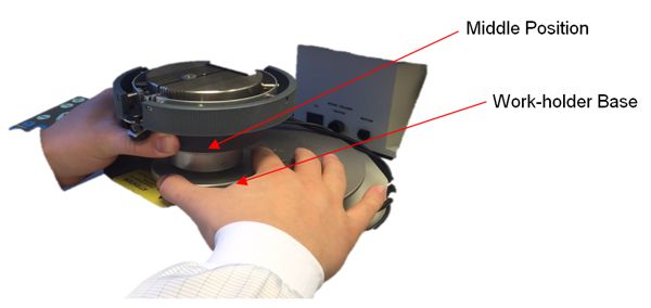
  5. Hold the work-holder static in the middle and by rotating the base the height can be adjusted.
    a. Rotate clockwise to raise workholder height.
    b. Rotate anti-clockwise to lower workholder height.
  6. Rotate workholder anticlockwise fully to lowest position.
  7. Load workholder (with product to bond).
  8. Position workholder under the bonding tool.
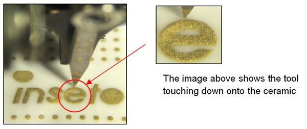
  9. Looking through the microscope raise work holder until lowest bonding surface is just touching the tool.
  10. Press the RESET button, the machine will now initialise.
  11. Increase the LOOP parameter to a higher value (4 – 5) to ensure good clearance above product.
  12. The work holder height is now setup correctly.
Manual Wire Bonder Workholder Setup
Workholder Height Adjustment
Manual Workholder Setup - Lower Position
Setup of Lower Worholder Height

Workholder Setup: Troubleshooting

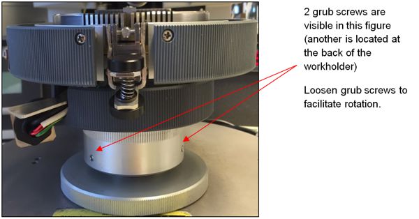
  • Problem: – The work-holder will not move in any direction (upwards or downwards).
  • Resolution: – The spring grub screws are too tight, loosen all 3 grubs screws slightly until rotation is possible.
Manual Workholder - Height Locking
Workholder Locking Adjustments

View the range of “MPP Equipment for Wire Bonding” (formerly KnS manual wire bonders).

Author

Date

Version

Author

Matt Houston

Date

28 April 2017

Version

IKB006 Rev. 3

Download

Author Biography

Matt Houston is a Sales Engineer at Inseto with over 16 years of experience in the microelectronics and semiconductor industry. His background spans process engineering, technical support and technical sales.

He began his career as a Process Engineer at C‑MAC in Great Yarmouth, working on die bonding and wire bonding for high‑reliability, high‑temperature electronic components, opto‑electronics and multi‑chip modules.

At Inseto, Matt has developed broad hands on experience across a range of semiconductor equipment through installations, training and process support. This enables him to support customers in selecting tailored solutions that meet specific technical requirements.

MPP & KnS NEFO Setup

3rd May 2020

Instructions on how to setup the position of the NEFO on all MPP and Kulicke and Soffa (K&S) Manual Wire Bonders (IKB-022).

NEFO Setup: Specific Precautions for Manual Ball Bonders with NEFO!

• Do not touch the NEFO wand of wire during bonding, NEFO Setup or when manually firing the Negative Electric Flame off (NEFO). The machine produces a HV spark between the NEFO electrode wand and the wire. This can cause an electric shock if contacted during the NEFO firing process. MPP recommend that people suffering from abnormal heart conditions or have pacemakers fitted do not operate or service the equipment.

• The NEFO wand assembly and circuit consist of a power supply circuit and a movable Wand (Electrode) that is actuated by a solenoid. When a FAB (Free Air Ball) is created at the end of the Ball Bonding cycle, the NEFO electrode is charged with a Negative HVDC charge and the NEFO solenoid pushes the Wand under the bottom tip of the capillary. The resulting spark passes from the wire to the Wand, melting the tail of the wire into a FAB. The NEFO Wand returns to its Wand Reset Position, ready for the next bonding cycle.

NEFO Adjustments

The flame-off wand needs to be adjusted for Gap (Height), Reset Position, Over-Travel and for Lateral Position.

Gap (Height):

To adjust the Gap between the Wand and the wire.

  • Turn on the Bonder and make sure the Bonder is in the Reset position (1st Bond indicator illuminated).
  • Loosen the NEFO Lock Screw.
  • Turn the Top Height Adjustment Screw until the NEFO Wand is at the recommended distance underneath the Capillary tip.
  • Tighten the Wand Lock Screw.

A rule of thumb is the greater the Gap the smaller the FAB (ball), increasing the Gap will also add more inconstancy to (FAB ball) sizes.

Recommend Flame-Off Gap Settings
Recommended NEFO Gaps Settings (Wire Size Dependent)

NEFO Gap
NEFO Example Gap (Capillary to NEFO)

Reset Position:

  • To adjust the NEFO Reset Position.
  • Loosen the NEFO Wand Solenoid Clamping Screw.
  • Turn the solenoid so that the NEFO Wand is close to, but not touching, the capillary during the bonding operation. (Note. The NEFO wand may slightly touch the Ultrasonic Bonding Arm during over-travel).
  • Tighten the NEFO Wand Solenoid Clamping Screw.

Over-Travel:

  • To Adjust the NEFO Wand Over-travel.
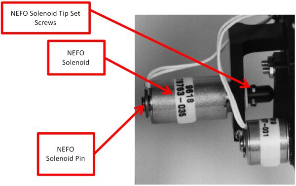
  • Loosen the NEFO Solenoid Tip Set Screws (x2)
  • Press the NEFO Solenoid Pin with your finger until the Circlip is fully pressed against the NEFO Solenoid Body.
  • Move the NEFO Solenoid Tip with the NEFO Wand until the NEFO wand protrudes past the bottom of the capillary by 1 – 1.5mm.
  • Tighten both NEFO Solenoid Tip Set Screws.

Solenoid Assembly
NEFO Solenoid Assembly

NEFO Reset Position
NEFO Over-Travel Position

Lateral Position:

  • To adjust the lateral position.
  • Loosen the NEFO Wand retaining Screws.
  • Tilt and manoeuvre the NEFO Wand until the Tip of the Capillary is central to the NEFO Wand.
  • Tighten the NEFO Wand Retaining Screws.

NEFO Lateral Alignment

View the range of “MPP Equipment for Wire Bonding” (formerly KnS manual wire bonders).

Author

Date

Version

Author

Adam Marshall

Date

17 November 2017

Version

IKB022 Rev. 1

Download

Author Biography

Adam Marshall is a Senior Technical Support Engineer at Inseto Ltd with over 14 years of experience in the semiconductor industry, including 10 years specialising in assembly processes and related equipment. He supports customers across the microelectronics and semiconductor sectors who rely on precision equipment to maintain reliable and repeatable results in production and research environments.

Known for a calm and structured approach, Adam works closely with customers, suppliers and internal teams to deliver clear technical advice and dependable support when it matters.

MPP & KnS 30/45 Degree Clamp Adjustments

3rd May 2020

Adjusting the 30/45 degree wire feed clamps on Micro Point Pro & Kulicke and Soffa (K&S) Manual Wire Bonders (IKB-021).

In order to correctly setup 30/45 degree wire clamps to the factory standard please follow the procedures below carefully.

Clamp Solenoid Assembly Replacement:

  1. Follow the cables from the clamp solenoid to inside the machine. Open the left door to find a connector, which connects the clamp solenoid to a harness cable which is plugged into the logic board, found at the rear of the machine.
  2. Disconnect the solenoid from the connector and remove the harness from all metal clamps holding it to the bonding head.
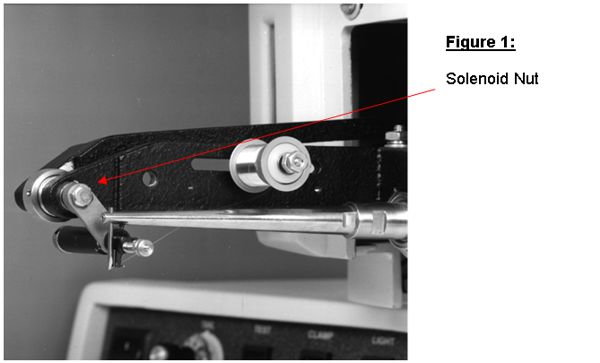
    1. Using a 1/4″ open wrench, unscrew the solenoid nut (see figure 1). Remove the clamp assembly.
  3. To install a new solenoid assembly, perform the opposite action in step 2.
  4. Reconnect the solenoid to the connector.
30/45 Degree Clamps Setup #1

Clamp Position Adjustment:

Once the new clamp assembly is fitted to the machine, if the angle of the clamp face does not look like the image (parallel to the bonding wedge) or similar, adjustments need to be made.

If adjustments are required:

  1. Remove the solenoid nut (see figure 1).
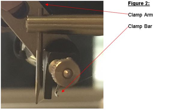
  2. The clamp assembly can now be unscrewed, do this by holding the clamp arm and rotating the solenoid in an anti-clockwise rotation.
  3. Position the clamp to the correct angle; keep checking against the tool until the desired position is met.
  4. The gap between the back of the wedge and the front of the clamps should be approx. 1mm. The gap between the bottom of the wedge and the bottom of the clamps should also be approx. 1mm.
  5. Once the correct position is achieved, tighten the solenoid against the clamp arm (see figure 2), place the assembly into position and tighten the solenoid nut.
  6. Place the wire through the clamps and push the clamp bar close to the clamps, so it is almost touching. This will prevent the wire from slipping out of the clamps during bonding.

30/45 Degree Clamps Setup #2

Clamp Force Adjustment:

To setup the correct clamping force for the new clamps:

  1. Open the clamp using the CLAMP switch/button.
  2. Feed some wire between the two clamp faces.
  3. Close the clamp using the CLAMP switch/button.
  4. Pull the wire carefully using tweezers; if the wire breaks cleanly then the clamp force is setup correctly. Otherwise follow the next few steps.
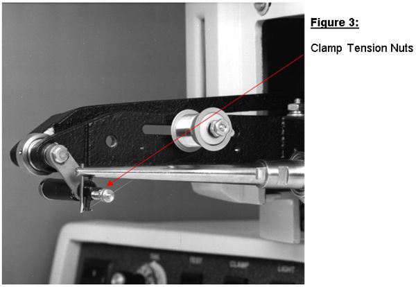
  5. Loosen both clamp tension nuts from the side of the clamp until they are at the end of travel (see figure 3). The right-most nut is for locking the position of the left-most nut, which presses against the spring and provides tension to the clamp.
  6. Repeat steps 1 – 4, however, turn the nuts clockwise (towards the solenoid) until the wire breaks cleanly.

30/45 Degree Clamps Setup #3

Clamp Lateral Position Adjustment

  1. The wire path must be a straight line from the transducer hole to the wedge feed hole. The wire clamp leads the wire from the wedge feed hole to the wedge foot. If the clamp and the wedge feed hole are not aligned along the same axis, the wire will not be centered under the foot of wedge. This results in bonding inconsistencies.
  2. To adjust the clamp lateral position:
    1. Feed the wire through the clamp jaws and the wedge feed hole. Focus the microscope on the tip of the wedge and check if the wire is in the centre of the wedge. If it is, exit the procedure at this point.
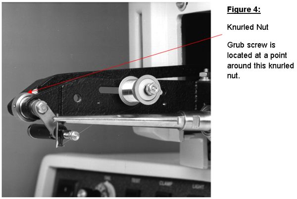
    2. Loosen the set screw that faces you (see Figure 4). Adjust the clamp’s lateral position by turning the knurled adjusting nut so that the wire is centred under the wedge foot.
  3. Perform a few bonds and check that the wire is still centred. If necessary, adjust the clamp’s lateral position more.
  4. Secure the knurled adjusting nut by tightening the set screw.

30/45 Degree Clamps Setup #4

View the range of “MPP Equipment for Wire Bonding” (formerly KnS manual wire bonders).

Author

Date

Version

Author

Matt Houston

Date

04 July 2017

Version

IKB021 Rev. 1

Download

Author Biography

Matt Houston is a Sales Engineer at Inseto with over 16 years of experience in the microelectronics and semiconductor industry. His background spans process engineering, technical support and technical sales.

He began his career as a Process Engineer at C‑MAC in Great Yarmouth, working on die bonding and wire bonding for high‑reliability, high‑temperature electronic components, opto‑electronics and multi‑chip modules.

At Inseto, Matt has developed broad hands on experience across a range of semiconductor equipment through installations, training and process support. This enables him to support customers in selecting tailored solutions that meet specific technical requirements.

MPP & KnS Deep Access Clamp Adjustments

3rd May 2020

Adjusting deep access wire clamps (90 degree feed) on Micro Point Pro & Kulicke and Soffa (K&S) Manual Wire Bonders (IKB-007).

• Adjust deep access (90° feed) clamps with machine switched on.

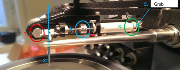
Manual Wire Bonder - Deep Access Clamp Adjustments: MPP and KnS
45XX Series Manual MPP and K&S Wire Bonder – Deep Access Clamp Adjustments

1. Red Circle Lateral Position Adjustment
This locking nut holds the clamp assembly in place. Loosen using a 1/4” spanner to perform any lateral adjustments to the clamp.

2. Blue Line – Clamp to Tool Alignment
Align the rear fixed clamp (with clamp held open) to the tool hole. Align the rear clamp such that the wire does contact the fixed clamp; this will allow straight, drag free motion in the wire during bonding. The clamp assembly should be perpendicular to the bonding tool.

3. Green Circle – Solenoid to Transducer Distance
Set TAIL dial to 10 to lower the clamp arm to minimum. Adjust the clamp assembly such that the solenoid body is as close as possible to the transducer without touching (approx. 1 – 2 mm). Tighten the locking nut (red circle) to secure the assembly.

4. Blue Circle – Clamp Force Adjustment
Loosen the rear locking nut. Adjust the force setting via the front sprung nut. The compressing spring will increase the closed clamp force. Adjust the force so the wire breaks cleanly without slipping through the closed clamps.

5. Grub Screw – Clamp Gap Adjustment
Loosen the 2 x grub screws on the gap plate on the rear of the solenoid. Push the solenoid rod (with clamps closed) forward until the desired clamp gap is achieved. Tighten the grub screws. Test the solenoid operation using the CLAMP toggle switch on the machine. The clamp gap is typically set to 2 – 3 wire diameters.

View the range of “MPP Equipment for Wire Bonding“.

Author

Date

Version

Author

Matt Houston

Date

28 April 2017

Version

IKB007 Rev. 5

Download

Author Biography

Matt Houston is a Sales Engineer at Inseto with over 16 years of experience in the microelectronics and semiconductor industry. His background spans process engineering, technical support and technical sales.

He began his career as a Process Engineer at C‑MAC in Great Yarmouth, working on die bonding and wire bonding for high‑reliability, high‑temperature electronic components, opto‑electronics and multi‑chip modules.

At Inseto, Matt has developed broad hands on experience across a range of semiconductor equipment through installations, training and process support. This enables him to support customers in selecting tailored solutions that meet specific technical requirements.

MPP & KnS How to Measure Static Bond Force

3rd May 2020

How to measure the static load applied by the bond tool on Micro Point Pro & Kulicke and Soffa (K&S) manual wire bonders (IKB-008).

The static bond force is the force that is applied to the bonding wedge or capillary when the force dial is set to zero and no external force is provided from the force coil during bonding. Typically when bonding 25 micron wire the static force should equate to:

  • 15 – 18 grams for Wedge bonding.
  • 23 – 25 grams for Ball bonding.

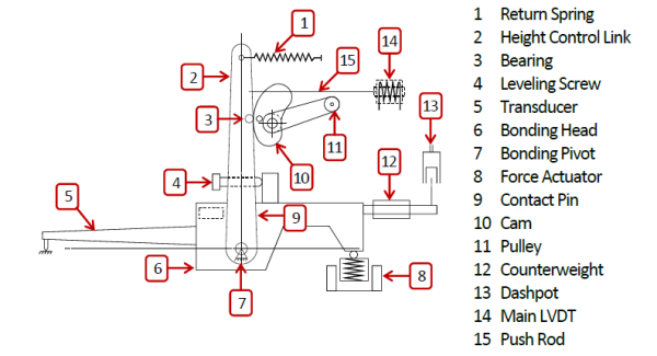
Larger or smaller wire diameters will require additional or lower static force respectively. The static force is adjusted with two counter balance weights on the rear of the bond arm. One is located near the dashpot assembly (left) and the other is located near the bond head pivot (right). If higher bonding force is required, one or both of these counter balance weights can be removed.

Adjust Static Bond Force:

• Isolate bonder.

• Open right hand side cover and remove the return spring from one end; this will allow the bond head and transducer assembly to naturally fall to the end of its travel.

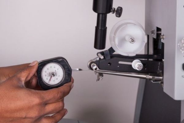
• Place a suitably scaled Gram Gauge under the wedge / capillary.

• Adjust the counter balance weights until you have a suitable static bond force.

• Reconnect return spring and close covers.

MPP and K&S Manual Wire Bonder - Static Bond Force Adjustment
MPP & KnS Manual Wire Bonder Adjustments

Static Bond Force Measurement
MPP & KnS Manual Wire Static Force Measurement

View the range of “MPP Equipment for Wire Bonding” (formerly KnS manual wire bonders).

Author

Date

Version

Author

Adam Marshall

Date

22 May 2017

Version

IKB008 Rev. 3

Download

Author Biography

Adam Marshall is a Senior Technical Support Engineer at Inseto Ltd with over 14 years of experience in the semiconductor industry, including 10 years specialising in assembly processes and related equipment. He supports customers across the microelectronics and semiconductor sectors who rely on precision equipment to maintain reliable and repeatable results in production and research environments.

Known for a calm and structured approach, Adam works closely with customers, suppliers and internal teams to deliver clear technical advice and dependable support when it matters.

Ball Bond Sequence

3rd May 2020

Explanation of the ball bonding cycle for ultrasonically welding electrical interconnects in microelectronics (IKB-001).

The Ball Bond sequence for both manual and automatic wire bonding machines can be explained in seven steps:

Ball Bond Sequence
Ball Bond Sequence

  • STEP 1: BALL FORMATION: Spark from EFO wand melts wire to form ball for first bond.
  • STEP 2: FIRST BOND: Ball bond ready to commence. Tool brought over first bond position (X, Y) and down into contact with surface – force is pre-set value – ultrasonic energy applied for pre-set time to form first bond.
  • STEP 3: LOOP HEIGHT: Tool is raised to pay wire out from spool (clamps open) to loop height value.
  • STEP 4: LOOP FORMATION: Tool moved to second bond position (manually or automatically).
  • STEP 5: SECOND BOND: Tool brought into contact with surface – second bond made as step 2.
  • STEP 6: TERMINATION: Following 2nd bond, tool moves up to pre-set height (tail), clamps close and break off wire at 2nd bond heel.
  • STEP 7: BALL FORMATION: Automatic repeat of step 1 to begin cycle again.

View the range of “MPP Equipment for Wire Bonding“.

View the range of “K&S Automatic Wire Bonders“.

View the range of “Coining Wire Bonding Materials“.

View the range of “K&S Wire Bonding Capillaries“.

Author

Date

Version

Author

Jim Rhodes

Date

22 May 2017

Version

IKB001 Rev. 3

Download