Inseto

Month: May 2020

Fine Wire Wedge Bond Sequence

3rd May 2020

Wedge Bond Sequence: Explanation of the fine wire wedge-wedge bonding cycle to ultrasonically weld electrical interconnects in microelectronics (IKB-002).

The fine wire wedge bond sequence for both manual and automatic equipment can be explained in eight steps:

Wedge Bonding Sequence

  • STEP 1: RESET / REST / IDLE: Wire is located under the bonding tool between surfaces (chip or lead).
  • STEP 2: FIRST SEARCH: Tool descends to first bond search height for final positional (X, Y) adjustment.
  • STEP 3: FIRST BOND: Tool brought into contact with surface – force is pre-set value – ultrasonic energy applied for pre-set time to form first bond weld.
  • STEP 4: LOOP HEIGHT: Tool is raised to pay wire out from spool (clamps open) to pre-set loop height value.
  • STEP 5: LOOP FORMATION: Tool steps back to second bond position (manual or automatic).
  • STEP 6: SECOND SEARCH: Tool descends to second bond search height for final positional (X, Y) adjustment.
  • STEP 7: SECOND BOND + TERMINATION: Tool brought into contact with surface – second bond made as stage 2.
  • STEP 8: TAIL FEED: Following 2nd bond, clamps close and break off wire at bond heel (or via table tear). Wire is then fed back under the tool (tail) for next bond.

View the range of “MPP Equipment for Wire Bonding“.

View the range of “K&S Automatic Wire Bonders“.

View the range of “Coining Wire Bonding Materials“.

View the range of “MPP Bonding Wedges“.

Author

Date

Version

Author

Jim Rhodes

Date

05 April 2017

Version

IKB002 Rev. 4

Download

Bond Wire Handling Considerations

3rd May 2020

Bond Wire Handling: A guide on how to correctly handle and store bonding wire (IKB-023).

Bond Wire Storage:

Wire Bonding in the Electronics Industry is typically carried out using either Gold (Au), Silicon / Aluminium (1%SiAl), Aluminium (99.99% or 99.999%), or Copper (Cu), with diameters ranging from 12.5µm to 500µm. Ribbon is also used in a variety of sizes for low impedance / high frequency applications.

It is very important to store this wire in accordance with the manufacturer’s recommendations. Typically bond wire will have a shelf life, because while the build-up of oxides can be reduced, it cannot be fully eliminated. This is especially true for aluminium and copper wires.

Typical storage instructions would be to store the wire spools in a humidity controlled cabinet and away from direct heat. Spools should never be spooled on their edges, as this may causing de-spooling.

Bonding wire is usually spooled from one end of a spool to the other in a single layer. Each end is usually secured to the edge of the spool with a piece of coloured tape. Each end of the wire will have a different colour indicating the start and the end of the spool. It is important when starting a new spool to check the manufacturer’s instructions on what end is the beginning, this information will usually be on the packaging of the wire spools.

Wire bonding fine wire is usually supplied in two spool types, 0.5 inch diameter spools and 2 inch diameter spools.

Wire Spool Handling:

One of the most common process challenges to overcome in wire bonding is contamination. Any organic contamination can seriously affect the consistency and quality of wire bonding. So it vital that the wire and any items that touch the wire are clean and free from contaminants such as oil from fingertips.

It is necessary to wear gloves or finger cots while handling the wire during threading and also to ensure tools such as tweezers are clean – this will help eliminate cross contamination. Alcohol may be used to clean any parts / tools that have direct contact to the wire.

Bond Wire Spool Storage Technique
Wire Bond Footprint

View the range of “Coining Wire Bonding Materials“.

Author

Date

Version

Author

Adam Marshall

Date

15 June 2017

Version

IKB023 Rev. 1

Download

Author Biography

Adam Marshall is a Senior Technical Support Engineer at Inseto Ltd with over 14 years of experience in the semiconductor industry, including 10 years specialising in assembly processes and related equipment. He supports customers across the microelectronics and semiconductor sectors who rely on precision equipment to maintain reliable and repeatable results in production and research environments.

Known for a calm and structured approach, Adam works closely with customers, suppliers and internal teams to deliver clear technical advice and dependable support when it matters.

MPP Bonding Wedge Tool Nomenclature

3rd May 2020

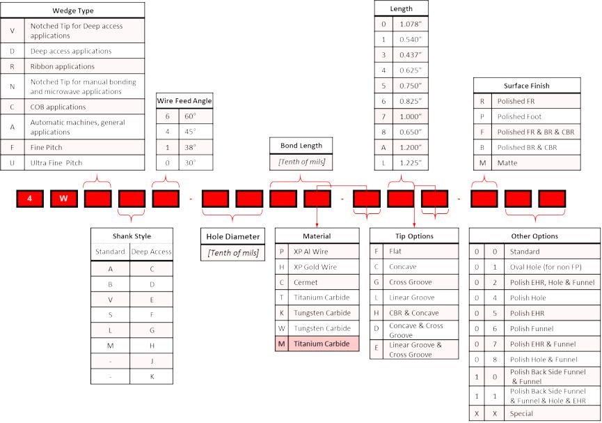
Bonding Wedge Tool Nomenclature: This article explains the nomenclature used to identify Micro Point Pro’s bonding tools for wire and ribbon bonding (IKB-010).

Bonding wedge tool selection is key to a successful and stable wire bond process. Bonding tools are high precision manufactured, with attributes specific to the wire diameter in use and bonding process parameters.

Bonding wedge tools are manufactured from three main materials:

  • Tungsten Carbide for aluminium wire
  • Titanium Carbide for gold wire
  • Ceramic tipped tungsten carbide tools are also available for gold processes

The figure below describes the Micro Point Pro round wedge nomenclature:

MPP - Bonding Wedge Tool Nomenclature
MPP Bond Wedge Tool Nomenclature

Three main selection criteria for the above bond wedges are:

Hole Diameter (H):
This contributes to bond placement accuracy and wire clearance during looping.

Hole Angle (Ha):
This contributes to looping consistency, heel stress in the bonds and tailing consistency.

Bond Length (BL):
Directly affects 1st / 2nd bond size, wire pull strength.

Wedge Bonding Tool Foot Criteria
Wedge Tool Critical Dimension Nomenclature

View the range of “Bonding Wedge Tools“.

View the range of “Coining Wire Bonding Materials“.

View the range of “MPP Equipment for Wire Bonding“.

View the range of “K&S Automatic Wire Bonders“.

Author

Date

Version

Author

Jim Rhodes

Date

11 August 2017

Version

IKB010 Rev. 1

Download

Semiconductor Wafer Nomenclature

3rd May 2020

This article explains the nomenclature used to identify our semiconductor wafer types and specifications, along with the key descriptive criteria to consider when choosing wafers (IKB-044).

Semiconductor wafer selection is key to a successful use of wafers and substrates for your process. Wafers are manufactured with very high precision, with attributes specific to the electronic and mechanical properties and any coatings applied after manufacture.

Wafers are manufactured from four main materials:

  • Silicon
  • Glass and Fused Quartz
  • 3-5 or 2-6 Compound Semiconductors
  • Sapphire

The figure below describes Inseto’s nomenclature chart for Silicon wafers:

Silicon Wafer Nomenclature
Silicon Wafer Nomenclature Chart

The second category of wafers we classify is coated wafers. These are wafers with an added layer either on both the top and bottom surfaces of the silicon or just one of the surfaces – usually the top.

The figure below shows Inseto’s nomenclature chart for Coated Wafers:

Oxide and Nitride Coated Wafer Nomenclature
Oxide and Nitride Coated Wafer Nomenclature Chart

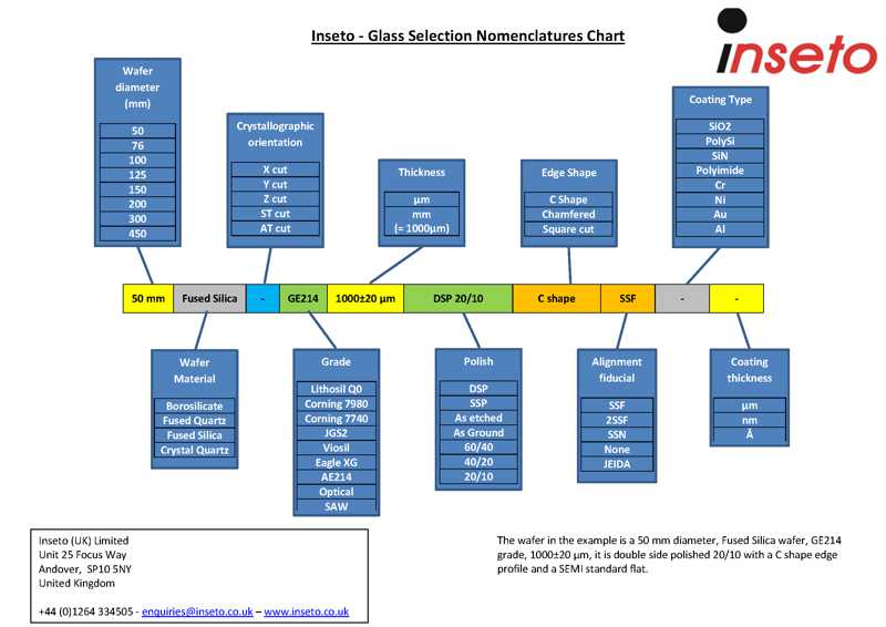
The third category of wafers we classify is glass wafers. These are used when a transparent substrate is required and are categorised by a different set of parameters.

The figure below shows Inseto’s nomenclature chart for Glass Wafers:

Glass Wafer Nomenclature Chart

The fourth category we use to classify our wafers is SOI wafers or Silicon-on-Insulator.

These wafers are a sandwich of silicon-insulator-silicon. The insulator is typically silicon oxide or sapphire and the make-up of these is highly specific to the end application.

The figure below shows Inseto’s nomenclature chart for SOI Wafers:

Silicon-on-Insulator SOI Wafer Nomenclature Chart
SOI (Silicon-on-Insulator) Wafer Nomenclature Chart

The fifth category we use to classify our wafers is as SOS – Silicon-on-Sapphire.

These wafers have an EPI Silicon layer on Kr grown Sapphire Wafers. The figure below shows Inseto’s nomenclature chart for SOS Wafers:

SOS Wafer Nomenclature
SOS (Silicon-on-Sapphire) Wafer Nomenclature Chart

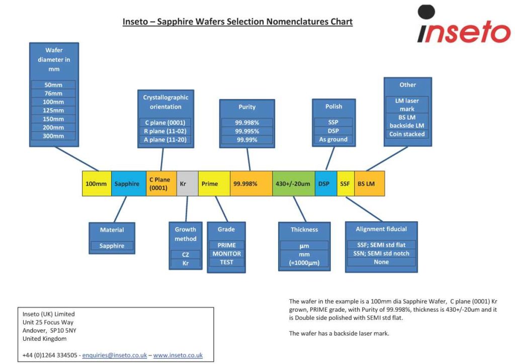
The final category we use to classify our wafers is Sapphire.

These wafers are prime grade high quality with C, A and R plane crystal orientation from 2″ to 150mm. They are Single or double side polished have low roughness and are defect free.

The figure below shows Inseto’s nomenclature chart for Sapphire Wafers:

Sapphire Wafer Nomenclature
Sapphire Wafer Nomenclature Chart

Author

Date

Version

Author

Ian Burnett

Date

26 March 2019

Version

IKB044 Rev. 4

Download

Solder Reflow Using Formic Acid

2nd May 2020

Explanation of the fluxless vacuum solder reflow process using formic acid for oxide reduction (IKB-017).

Traditionally solder reflow has been used with a liquid flux additive, to further increase the wetting of solder to metals with high oxide layers. There are, however, flaws or issues that come with using flux in your soldering process.

Voiding:
Because all flux has a liquid component it is prone to out-gassing and vaporising during the elevated temperatures of the soldering process. This out-gassing is the cause for voiding (trapped gas) between two soldered surfaces. An example can be seen when soldering high power semiconductors. During die attach, where heat transfer is crucial to the performance of both the die and the end-product, voiding can cause localised heat spots on a die’s surface, leading to stress and fatigue cracks. Although the addition of soldering under vacuum further reduces the voiding, it is still not considered ideal.

Flux Residue:
Soldering with flux naturally leaves residue and then you are left with the process of removing and cleaning your part. Follow-on processes such as wire bonding require clean parts, free from contamination, so the cleanliness is critical. Flux residue is also known to react with water vapour to create an acidic solution on the surface of parts. This can affect the long term reliability of your devices.

Flux-Free Reflow:
The ideal solution is to perform the soldering process in a flux-free atmosphere. Soldering in a 100% Hydrogen atmosphere is one method used for flux-free soldering that removes surface oxides. This adds an explosive risk and is dangerous; the equipment needed would need to be ATEX approved. Forming gas (a mix of Nitrogen and Hydrogen, 90% – 10% respectively) is safer, but the effective temperature is equal to and above 350°C, which is not compatible with the lower melting point solders.

Formic Acid Reflow:
A suitable alternative for flux-free soldering with lower temperatures is to perform the solder reflow under a formic acid (HCOOH) vapour. The vapour chemically reacts with the metal oxides at a lower temperature (150 – 160°C) to create formats; increasing the temperature even more decomposes the formats into Hydrogen, Water & Carbon Dioxide. When combined with a vacuum solder reflow system, these gases and vapours can be removed through the vacuum system.

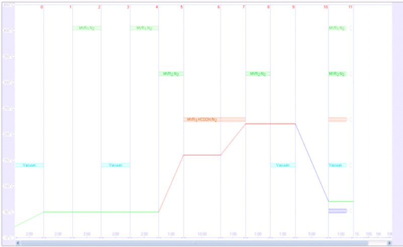
A typical formic acid vacuum solder reflow profile can be seen below. After two vacuum stages with nitrogen refill, the chamber is free from atmosphere and oxygen. The temperature is increased with the introduction of formic acid vapour (nitrogen is used as a carrier for the formic acid vapour) with a dwell at 160°C, and a further ramp up to 220°C with a dwell provides time for the solder reflow and oxide removal. The chamber is then purged with nitrogen and evacuated with the vacuum stage to remove any voiding.

Formic acid solder reflow is a proven method for flux-free soldering, and because the oxide removal properties of formic acid vapour are effective at lower temperatures, it is also a very flexible process. It eliminates the need for pre-reflow fluxing and post-reflow flux removal. And because of the corrosive properties of formic acid, it leaves bare metallic surfaces suitable for further diffusion processes such as wire bonding.

Formic Acid Solder Reflow Profile
Typical Solder Reflow Profile Using Formic Acid

For more information on our range of ATV Vacuum Solder Reflow Equipment, please click HERE.

Author

Date

Version

Author

Adam Marshall

Date

02 November 2017

Version

IKB017 Rev. 2

Download

Author Biography

Adam Marshall is a Senior Technical Support Engineer at Inseto Ltd with over 14 years of experience in the semiconductor industry, including 10 years specialising in assembly processes and related equipment. He supports customers across the microelectronics and semiconductor sectors who rely on precision equipment to maintain reliable and repeatable results in production and research environments.

Known for a calm and structured approach, Adam works closely with customers, suppliers and internal teams to deliver clear technical advice and dependable support when it matters.

Wafer Probe Tip Selection

2nd May 2020

A guide on wafer probe tip selection (IKB-034).

Probe Tips – sometimes referred to as Probe Needles – come in a variety of materials, lengths, shapes and tip radii.

They provide direct electrical contact to the circuit under test.

Probe Tips are specified to suit each individual application; considerations should be made regarding the material to be probed, temperature, bond pad size and bond pad thickness.

Probe Tips usually come in a variety of materials to suit individual applications:

Nickel Shank – Tungsten Tipped
(0.1µm – 1.0µm)

Submicron probe for small feature probing – can easily to be bent or cut to length.

Tungsten Shank – Tungsten Tipped
(0.06µm – 25.0µm)

General purpose probing.

Tungsten Shank and Tip – Gold Plated
(5.0µm – 50.0µm)

For probing gold contacts and pads – reduced contact impedance.

Tungsten Carbide Shank – Tungsten Carbide Tip
(5.0µm – 25.0µm)

Suitable for high temperature operation.

Beryllium Copper Shank – Beryllium Copper Tip
(5.0µm – 20.0µm)

Reduced contact impedance – suitable for probing soft materials, reduced pad damage.

Probe Tips with a larger radius will provide a lower impedance contact but have a larger footprint, although larger radius tips may be affected by any oxide contaminant layer on the contact pad. In this case, smaller radius tips will be sharper and able to pierce through to the contact material, whether this is Gold, Aluminium, Nickel or Copper. This compromise needs to be considered and chosen to suit the contact area available.

For more information on our range of Probe Station testing accessories please click HERE.

Author

Date

Version

Author

Adam Marshall

Date

27 June 2017

Version

IKB034 Rev. 1

Download

Author Biography

Adam Marshall is a Senior Technical Support Engineer at Inseto Ltd with over 14 years of experience in the semiconductor industry, including 10 years specialising in assembly processes and related equipment. He supports customers across the microelectronics and semiconductor sectors who rely on precision equipment to maintain reliable and repeatable results in production and research environments.

Known for a calm and structured approach, Adam works closely with customers, suppliers and internal teams to deliver clear technical advice and dependable support when it matters.

Annular Dicing Blade Selection

2nd May 2020

Annular Dicing Blade Selection: Choosing the right blade for your application is crucial to the success of your dicing process. The following information will help you understand the key parameters for selecting the correct dicing blade (IKB-036).

This document focuses on the “annular dicing blade” (also known as hubless) type; key parameters for selection are :

Blade Type: Annular Blades

Binder material: Nickel, Resin, Sintered Metal or Steel Cored

Blade Dimensions: Inner Diameter, Outer Diameter and Thickness

Edge Geometry: Standard, Serrated or Shaped

Abrasive Compound: Diamond, SiC, CBN, Grit size and Concentration

Matrix: Hard, Medium or Soft

Nickel Blades:
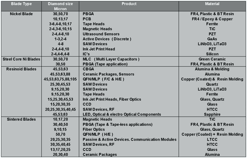
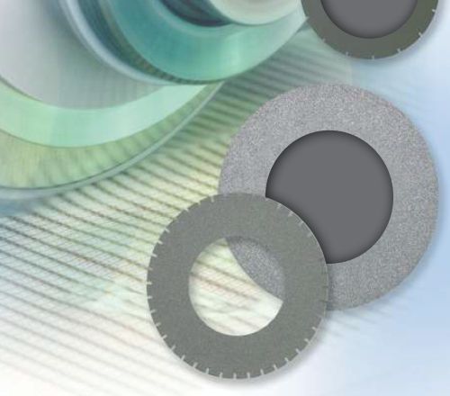
The nickel binder provides longer blade life and lower wear rate, and combined with the abrasive makes nickel-bond blades a perfect choice for soft material applications such as: PCB, PZT, Silicon and BGA (tape process).
Nickel blades consist of a uniform mixture of nickel and diamonds.
Blade thickness varies from 20 microns (0.8 mil) to 500 microns (20 mil), depending on diamond grit size and blade OD.
Diamond grit size ranges from 2-4 microns to 70 microns, depending on blade thickness.

Resin Blades:
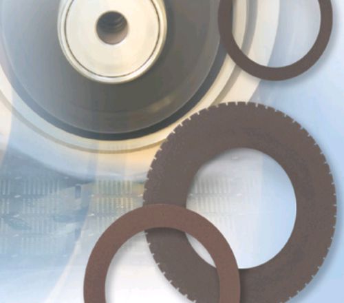
Resin as binder allows for blade wear management rendering resin-bond blades an excellent choice for hard and brittle materials such as: QFN/MLF, Thick Ceramic Substrates, HTCC and Glass.
Blade thickness varies from 75 microns (3 mil) to 2,500 microns (100 mil), depending on diamond grit size and blade OD.
Diamond grit size ranges from 3 microns to 250 microns, depending on blade thickness.

Sintered Metal Blades
With slower wear rate than resin but faster than nickel, sintered blades are best suited for retaining package shape and size in applications such as: BGA, Soft Alumina, LTCC and HTCC.

Blade thickness varies from 100 microns (4 mil) to 1,500 microns (60 mil), depending on diamond grit size and blade OD.
Diamond grit size ranges from 2 microns to 70 microns, depending on blade thickness.

Annual Dicing Blade Application Chart
Resin Bond Dicing Blades
Resin Bond Annular Dicing Blade
Nickel Bond Annular Dicing Blades by ADT
Nickel Bond Annular Dicing Blade
Metal Sintered Dicing Blades
Nickel Bond Annular Dicing Blade
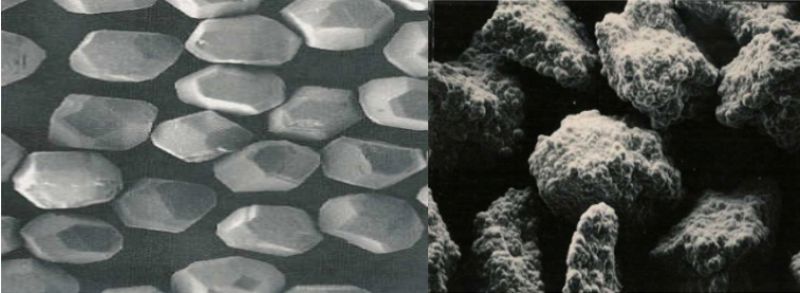
Diamond Concentrations in Dicing Blades
Diamond Concentrations

For further information on our range of dicing blades for annular mounted applications, please click HERE.

Author

Date

Version

Author

John Govier

Date

15 June 2017

Version

IKB036 Rev. 2

Download

Bonding Wire Sizes and Selection

1st May 2020

Bonding Wire Selection: What considerations are needed to be taken into account when selecting a wire for wire bonding? (IKB-037)

Selecting the correct bonding wire is critical to achieving reliable, repeatable wire bonds in microelectronics assembly. Wire choice directly affects bond quality, electrical performance, long‑term reliability, and process stability.

Wire choice is influenced by electrical requirements, bond pad geometry, bonding process capability, and material compatibility.

Key Selection Criteria:

When specifying a bonding wire, the following parameters must be defined and understood.

  • Wire diameter
  • Bonding wire materials & purity
  • Mechanical properties
  • Wire spool size

Each parameter influences both bond quality and process stability.

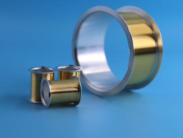
Example Gold Bonding Wire & Spool Types

Wire Diameter:

Bonding wire diameters typically range from 12.5 microns to 500 microns.

  • 12.5 to 75 microns
    Considered fine wire bonding, commonly used in general semiconductor and high-density applications.
  • 100 to 500 microns
    Considered large or heavy wire bonding, typically used for power devices, discrete components, battery connections and high current interconnects.

Wire diameter is usually determined by the circuit (such as current-carrying capability and frequency required) or component requirements and tolerances (such as bond pad size, pitch and length).

Wire pad size, position and pitch will greatly affect the constraints of the maximum wire diameter that can be used. The greater the outside wire diameter the larger the bonding tool will need to be, the larger the tool the more clearance is needed between bonds, directly affecting the minimum pitch size that can be bonded.  Other factors that will need to be considered are the fusing current, electrical resistance, thermal conductivity and active impedance for high frequency applications.

Diagram showing wire bond and bond pad terminology

Bonding Wire Materials & Purity:

Bonding wires are manufactured from metals with high electrical conductivity, using the highest purity materials that are precisely doped and annealed to achieve the required grain structure and mechanical properties.

Material selection is usually driven by process compatibility, electrical performance and cost. The most commonly used materials are:

  • Gold
  • Aluminium
  • Copper

Large aluminium bonding wire for heavy wire applications (typically 100 – 500 microns) and ribbon generally has a purity of either 99.99% or 99.999%.

Fine aluminium bonding wire (typically 17 – 75 microns) is an alloyed wire, containing 1% silicon (1%SiAl) in order to help prevent silicon migration from a bonded semiconductor die, which could result in a deterioration in bond quality and durability, as well as loop shape stability.

Gold bonding wire used in fine wire applications (typically 12.5 to 75 microns), is manufactured from 99.99 percent pure gold with controlled doping additives. These additives enable high speed automatic bonding and consistent bond and loop formation.

Other materials can be used and found in wire bonding for specific applications, examples of which are silver, platinum, palladium, and some coated wires. These materials are often selected for enhanced electrical performance, improved reliability, or reduced material cost.

Mechanical Properties:

The mechanical properties of bonding wire vary depending on the bonding process and application.

  • Tensile strength affects wire handling, bond pull strength, and resistance to deformation.
  • Elongation influences loop formation, stress absorption and resistance to fatigue during thermal cycling.

Different bonding processes, such as ball bonding, wedge bonding, and ribbon bonding, require different balances of tensile strength and elongation to achieve stable and repeatable bonds.

For example, the specification of a 25µm gold wire for a thermosonic ball bond is different from that needed to make a thermosonic wedge bond. As the looping profiles on a ball bond will be usually higher compared to a wedge bond, then having a wire that is stable at higher loops is more critical in your wire selection – the higher and more stable the wire is at looping could mean a compromise in strength and / or reliability. The 25µm gold wire that has been thermosonic wedge bonded will usually have lower loops that need to be stable and have lower impedance for high frequencies applications. The wire will be doped, annealed and tooled to suit these characteristics. Each desired criteria of the wire will affect the bonding performance in some way so research into the wire’s datasheet is essential.

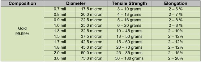
Example tables showing material composition and wire diameters with typical tensile strengths and elongations

Fusing Currents:

The fusing current is the minimum electrical current that heats a wire to its melting point, causing the conductor to fuse (break). It is a critical parameter for circuit protection and wire sizing, linking electrical loading to thermal failure limits.

Determining the fusing current helps engineers prevent overheating-related wire failures by accounting for material thermal and electrical properties.

Gold: Has superior corrosion resistance and high conductivity; cost and weight are limiting factors.

Aluminium: Lightweight and cost-effective. Lower conductivity than copper and gold, but suitable for large-scale power transmission.

Copper: Offers excellent electrical conductivity and mechanical strength but is more difficult to wire bond due to harder material properties and tendency to oxidise.

The following table of “Maximum Wire Bond Currents” is for indicative purposes only, based on wire lengths > 0.040”, and per Mil-H-38534.

Bonding Wire Fusing Current Table
Note: for indicative purposes only, users must verify their own results independently

Grain Structure:

Grain structure can affect the properties of the wire bond being made.

In power electronic circuits, grain boundary behaviour in aluminium wire bonds directly affects maximum continuous current capability, thermal cycling lifetime, resistance drift over life, and failure mode predictability. In ball bonding applications, during the ball formation, the grain structure of the wire directly above the FAB (free air ball) is altered. The heat affected zone (HAZ) is mechanically weaker than the original wire, so this directly affects the loop formation and stability. A fine grain structure introduces a shorter HAZ providing lower loop heights. A long HAZ assists in loop shapes that are naturally higher without relying on the capillary trajectory.

Example Diagram showing the ball bond heat affected zone (HAZ)

Wire Spool Size:

Correct spool choice helps maintain consistent wire feed and reduces the risk of handling damage or contamination.

There are two main considerations to consider when specifying what spool type you need for your bonding wire. The first is the spool type itself, which needs to be compatible with the wire bonding system you are working with. As the wires are subject to contamination which can affect bond quality and strength, as well as the fine nature of the wire, reworking or re-spooling the wire is not recommended, making the spool specification more critical.  

The second criterion to consider is the length of the wire required on the spool as well as how many layers being wound. Multi-wound spools that have more than one layer of wire wound onto the spool will hold an increased length of wire, but this increases the risk of wire becoming snagged from the spool as it is fed into the wire bonding machine. Fine wire SiAl is more prone to becoming snagged if oxide layers start to form from incorrect storage. This is especially true for small bobbin-like spools that have multiple wires, as this wire tends to have “memory” so it will try to return to the wound shape if left unused on the machine for too long.

For manual wire bonding machines, it is recommended to use a single wound layer to prevent this. If using a fully automatic wire bonder, then changing wire spools means additional down time which will affect production and throughput each time a machine is stopped for a spool change, so a multi-wound spool may be more desirable.

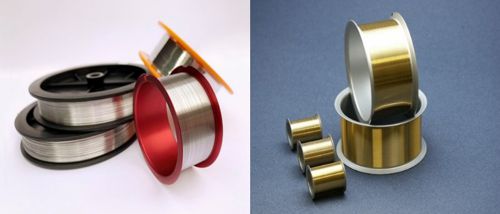
Exmple Inseto Bonding Wire and Spool Types
Exmple Bonding Wire and Spool Types
Inseto Bonding Wire Spool Descriptions
Example tables details the different spool types and their descriptions

Practical Selection Checklist

Before specifying a bonding wire, confirm the following:

  • Bond pad material, size, and pitch are compatible with the selected wire diameter
  • Electrical current and frequency requirements are met
  • Bonding equipment and tooling support the chosen wire material and size
  • Mechanical properties align with the intended bonding process
  • Environmental and reliability requirements are satisfied

Summary

Bonding wire selection is a balance between electrical performance, mechanical behaviour, process capability, and cost. Correct specification ensures reliable interconnects, stable bonding processes, and long-term device performance.

View the range of “Coining Wire Bonding Materials“.

Author

Date

Version

Author

Adam Marshall

Date

28 April 2020

Version

IKB037 Rev. 3

Download

Author Biography

Adam Marshall is a Senior Technical Support Engineer at Inseto Ltd with over 14 years of experience in the semiconductor industry, including 10 years specialising in assembly processes and related equipment. He supports customers across the microelectronics and semiconductor sectors who rely on precision equipment to maintain reliable and repeatable results in production and research environments.

Known for a calm and structured approach, Adam works closely with customers, suppliers and internal teams to deliver clear technical advice and dependable support when it matters.

Plasma Etch PE25-75 PLC Programming

1st May 2020

How to programme and control a PE25, PE50, PE75 using the PLC interface (IKB-047).

This document presumes the user is familiar with the Low Pressure Plasma process and the Plasma Etch Inc. Equipment.

WARNING: Only qualified and competent personnel should access these features. Improper configuration changes could cause the machine to malfunction.

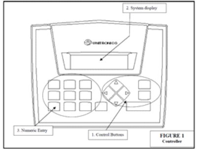
PLC Control Panel

The system controls and process are monitored through the front control/display panel keypad.

1. Control Buttons – System operation is controlled using these buttons.

2. System Display – Displays system messages, configuration information and machine status.

3. Numeric Keypad – Keypad for input for system setup.

NOTE:

  • Use the “left” and “right” arrow keys to find a menu item within a menu area.
  • Use the “up” arrow key to go to the previous menu area.
  • Use the “enter” key to select a menu item.

Operation & Programming Sequence:

1. Check and release the EMO if engaged.

2. Set the power circuit breaker to the On (Up) position.

3. The system will power up and once complete and ready will display the ‘Start up Screen’ – Machine Model and Firmware Version will be displayed.

4. Press the ‘Enter’ key to progress to the menus.

5. Pushing the ‘Left’ button will cycle between the ‘Setup’ and ‘Commands’ menu screens.

6. Cycle to ‘Setup’ and press ‘Enter’. System timer and other process variables will be found in this menu.

7. Using a combination of the ‘Numeric’ keys, ‘Control’ and ‘Enter’ keys, adjust the following relevant process variables to suit your process requirements:

A. Plasma Time – 0 – 59.59 mins. Amount of Plasma Process time required.

B. Vacuum Set Point – 1 – 1000mtorr. Vacuum level required before process gasses are introduced into the chamber.

C. Atmospheric Vent – 0 – 59.59 mins. Amount of time allowed for the chamber to vent to atmospheric pressure when ‘Cycle Stop’ is initiated. Variable dependent on Chamber size and if Atmosphere or N2 vent.

D. Purge Vent – 0 – 59 Seconds. Amount of time given for the purge Air or N2 to be introduced upon completion of a cycle.

E. Gas Stab – 0 – 59 Seconds. Once ‘Vacuum set-point’ is reached, this is the amount of time prior to ‘Plasma time’ to allow for the introduction of the process gasses and for the chamber pressure to settle in equilibrium.

F. Vacuum Alarm – 0 – 59.59 Seconds. Amount of time allowed for the pump to evacuate the chamber to the ‘Vacuum set-point’ before an ‘Alarm’ state is raised.

G. Auto Cycle Off – Off/On. Automatically goes into ‘Cycle off’ mode after cycle completion. (Shuts pumps off and vents Chamber.)

8. Access the ‘Commands’ Menu screen.

9. Load the Chamber- Take care not to ‘Short Circuit’ the electrode/shelf to the chamber walls.

10.0 Select the ‘Plasma’ Command and press ‘Enter’ to begin the sequence.

11.0 Observe the following:

I. The Vacuum Pump turns on and begins to evacuate the chamber.

II. The chamber vacuum reading will be displayed indicating the ‘Actual’ and ‘Vacuum set point’ values.

III. Once the ‘Vacuum set point’ has been reached the system will go into ‘Gas Stabilisation’.

IV. The ‘Gas Stabilisation’ allows the gases to stabilise for a period; this is defined in the ‘Gas Stab’ setting in the configuration menu. The following will be displayed: Gas Stabilize S: ** A: **

NOTE: Pressing the ‘Left’ Key at this point will display the current Chamber Vacuum level. This would have increased from the ‘Vacuum set point’ that had been achieved, due to the introduction of the process gases. To return to the ‘Gas Stabilisation’ screen, press the ‘Up’ key to return.

V. After the process gasses are stabilised, the RF power is enabled. The Wattage is determined by the Potentiometer dial on the front of the system.

VI. Inside the Chamber a Plasma Glow will be seen and the Plasma process timer will start. This was determined by the ‘Plasma Time’ in the commands menu.

VII. The following screen will be displayed: Plasma Time S: **.** A: **.**

NOTE: Pressing the ‘Left’ Key at this point will display the current Chamber Vacuum level. This would have increased from the ‘Vacuum set-point’ that had been achieved, due to the introduction of the process gases. To return to the ‘Plasma Time’ screen press the ‘Up’ key to return.

Using the commands menu the Plasma Time can be stopped short by using the ‘Cycle End’ Cue.

VIII. Once the ‘Plasma time’ is completed the RF power is removed, and the plasma glow will disappear from the chamber as the process gas valves are closed. The vacuum pump will shut off.

IX. Chamber Vent Valve is opened for the period determined in ‘Purge Vent – Purge Time’ in setup menu. This time dilutes any contaminants or harmful elements in the chamber before being evacuated by the vacuum pump again.

X. After completion of the ‘Purge Vent’ the chamber is evacuated by the pump until the ‘Vacuum set point’ is reached again.

XI. The process is complete

XII. If ‘Auto Cycle Off’ is ‘On’, the chamber will vent to Atmospheric pressure using the ‘Atmospheric Vent’ period determined in the setup menu. If ‘Auto Cycle Off’ is ‘Off’, the ‘Cycle Off’ cue will need to initiate using the commands menu.

XIII. The following message will be displayed: Plasma Cycle Complete.

The Chamber can now be opened.

For more information on Plasma Etch, plasma cleaning and etching equipment, please click HERE.

Author

Date

Version

Author

Adam Marshall

Date

25 March 2020

Version

IKB047 Rev. 1

Download

Author Biography

Adam Marshall is a Senior Technical Support Engineer at Inseto Ltd with over 14 years of experience in the semiconductor industry, including 10 years specialising in assembly processes and related equipment. He supports customers across the microelectronics and semiconductor sectors who rely on precision equipment to maintain reliable and repeatable results in production and research environments.

Known for a calm and structured approach, Adam works closely with customers, suppliers and internal teams to deliver clear technical advice and dependable support when it matters.